
Carbon nanotube transistors outperform silicon and GaAs
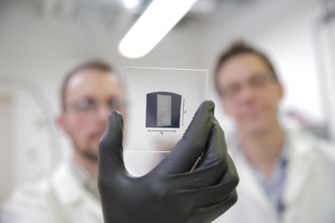
University of Wisconsin-Madison materials engineers have created semiconducting single-walled carbon nanotubes (CNTs) that outperform state-of-the-art silicon and GaAs transistors.
The researchers reported their advance in Science Advances in a paper titled 'Quasi-ballistic carbon nanotube array transistors with current density exceeding Si and GaAs'.
Led by Michael Arnold and Padma Gopalan, the team developed carbon nanotube transistors with a current 1.9 times higher than silicon transistors. The on-state current density exceeds that of GaAs FETs.
This breakthrough in CNT array performance is said to be a critical advance toward the exploitation of CNTs in logic, high-speed communications, and other semiconductor electronics technologies.
A 100nm channel length CNT array FET developed by the team had a current density of 900 mA mm-1 which they say exceeds the 630 mA mm-1 demonstrated by other researchers for GaAs pseudomorphic high-electron mobility transistor (pHEMT) technology.
"This achievement has been a dream of nanotechnology for the last 20 years," says Arnold. "This breakthrough in carbon nanotube transistor performance is a critical advance toward exploiting carbon nanotubes in logic, high-speed communications, and other semiconductor electronics technologies."
The new transistors are particularly promising for wireless communications technologies that require a lot of current flowing across a relatively small area.
Carbon nanotube transistors should be able to perform five times faster or use five times less energy than silicon transistors, according to extrapolations from single nanotube measurements. The nanotube's ultra-small dimension makes it possible to rapidly change a current signal traveling across it, which could lead to substantial gains in the bandwidth of wireless communications devices.
But researchers have struggled to isolate purely carbon nanotubes, which are crucial, because metallic nanotube impurities act like copper wires and disrupt their semiconducting properties - like a short in an electronic device.
The UW-Madison team used polymers to selectively sort out the semiconducting nanotubes, achieving a solution of ultra-high-purity semiconducting carbon nanotubes.
Placement and alignment of the nanotubes is also difficult to control. In 2014, the UW-Madison researchers overcame that challenge when they announced a technique, called "floating evaporative self-assembly," that gives them this control.
The nanotubes must make good electrical contacts with the metal electrodes of the transistor. Because the polymer the UW-Madison researchers use to isolate the semiconducting nanotubes also acts like an insulating layer between the nanotubes and the electrodes, the team "baked" the nanotube arrays in a vacuum oven to remove the insulating layer. The result: excellent electrical contacts to the nanotubes.
The researchers also developed a treatment that removes residues from the nanotubes after they're processed in solution.
"In our research, we've shown that we can simultaneously overcome all of these challenges of working with nanotubes, and that has allowed us to create these groundbreaking carbon nanotube transistors that surpass silicon and gallium arsenide transistors," says Arnold.
They are continuing to work on adapting their device to match the geometry used in silicon transistors, which get smaller with each new generation. Work is also underway to develop high-performance radio frequency amplifiers that may be able to boost a cellphone signal. While the researchers have already scaled their alignment and deposition process to 1 inch by 1 inch wafers, they're working on scaling the process up for commercial production.
The researchers have patented their technology through the Wisconsin Alumni Research Foundation.


