
Scientists integrate quantum dot micro-lasers on silicon
Results are major step towards direct III-V/Si epitaxy for integrating light sources on silicon
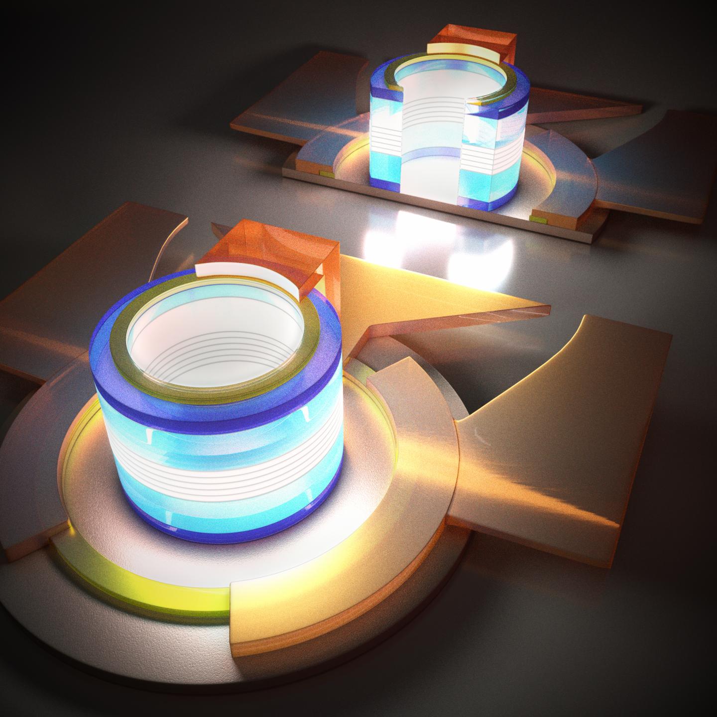
A group of researchers from the Hong Kong University of Science and Technology and University of California, Santa Barbara, have successfully demonstrated record-small electrically pumped micro-lasers epitaxially grown on industry standard (001) silicon substrates.
A submilliamp threshold of 0.6 mA, emitting at the near-infrared (1.3µm) was achieved for a micro-laser with a radius of 5 μm. The thresholds and footprints are orders of magnitude smaller than those previously reported lasers epitaxially grown on silicon. Their findings were published in Optica in August.
"We demonstrated the smallest current injection QD lasers directly grown on industry-standard (001) silicon with low power consumption and high temperature stability," said Kei May Lau, Fang Professor of Engineering and Chair Professor of the Department of Electronic & Computer Engineering at HKUST.
"The realisation of high-performance micron-sized lasers directly grown on silicon represents a major step toward utilisation of direct III-V/Si epitaxy as an alternate option to wafer-bonding techniques as on-chip silicon light sources with dense integration and low power consumption."
The two groups have been collaborating and has previously developed continuous-wave (CW) optically-pumped micro-lasers operating at room temperature that were epitaxially grown on silicon with no germanium buffer layer or substrate miscut. This time, they demonstrated record-small electrically pumped QD lasers epitaxially grown on silicon.
"Electrical injection of micro-lasers is a much more challenging and daunting task: first, electrode metallisation is limited by the micro size cavity, which may increase the device resistance and thermal impedance; second, the whispering gallery mode (WGM) is sensitive to any process imperfection, which may increase the optical loss," said Yating Wan, a HKUST PhD graduate and now postdoctoral fellow at the Optoelectronics Research Group of UCSB.
"As a promising integration platform, silicon photonics need on-chip laser sources that dramatically improve capability, while trimming size and power dissipation in a cost-effective way for volume manufacturability. The realisation of high-performance micron-sized lasers directly grown on Si represents a major step toward utilisation of direct III-V/Si epitaxy as an alternate option to wafer-bonding techniques," said John Bowers, deputy CEO of AIM Photonics.


