
Chengdu HiWafer chooses SPTS platform for GaN Line
Chinese pure-wafer foundry selects Omega plasma etch solution for production of high power RF devices
SPTS Technologies, an Orbotech company and supplier of wafer processing solutions, has won an order for its Omega plasma etch system from Chengdu HiWafer Semiconductor Co., Ltd (HiWafer), China's first pure-wafer foundry, to establish their new 6 inch GaN on SiC production line.
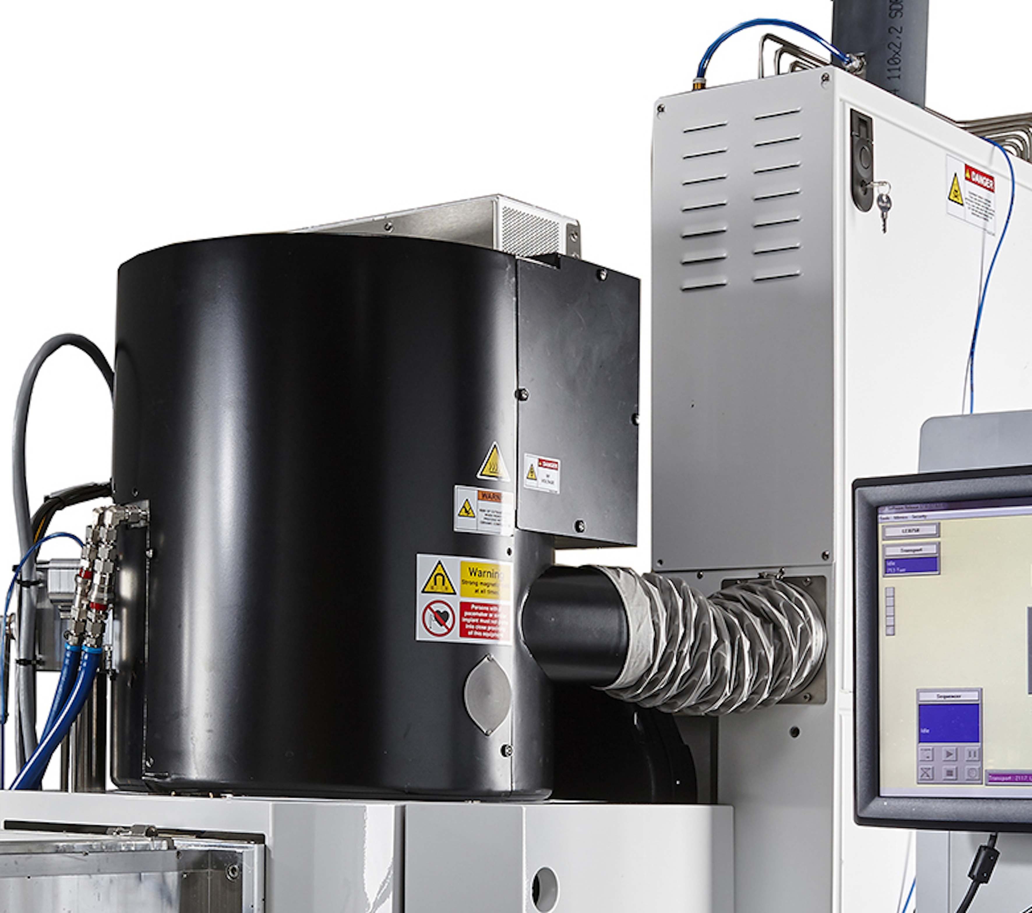
SPTS's Synapse and ICP process modules on an Omega c2L platform will etch SiC backside vias (BSV) and GaN epitaxial layers to manufacture high power RF devices. The high rate Omega system was selected over the competition because the Synapse provided superior SiC etch rates while the ICP module delivered improved selectivity for GaN etch.
"HiWafer is already a well-established Chinese foundry producer of GaAs based pHEMT and HBT RF devices currently used in 4G communication, and they are an early adopter of SiC and GaN materials for use in high-end RF devices that target the worldwide 5G protocol," stated Kevin Crofton, president of SPTS Technologies and corporate executive VP at Orbotech.
He added: "This leadership position is important as Power and RF applications are high on the "˜Made in China 2025' agenda for promoting domestic production of semiconductor devices, and companies like HiWafer are well-positioned to contribute to realising this national initiative. Our leadership in high rate etching of SiC and other dielectric materials will support HiWafer to provide manufacturing solutions for the coming 5G wave."
Nengwu Gao, general manager of HiWafer, stated: "Orbotech's SPTS Technologies is a recognised leader in compound wafer processing solutions to the global power and RF device industries. The addition of SPTS's Omega plasma etch system gives us the tools to compete in GaN on SiC RF technology in telecoms and transportation applications, including railway systems. Acquiring this capability enables us to explore new applications and supports our ambitions to become a highly profitable and successful semiconductor foundry."


