
KAUST and SMI show one-step tuning of Gallium Oxide phases
HCl-enhanced MOCVD approach could pave the way to low-cost, large scale hetero-epitaxy of Ga2O3 films with different phases for optical and power devices
Gallium oxide (Ga2O3) is attracting increasing attention due to its extremely high theoretical breakdown field of ~8 MV/cm which is several times higher than SiC (3 MV/cm) and GaN (3.8 MV/cm), suiting it to high power electronics.
Furthermore, due to its large intrinsic bandgap (4.5-5.1 eV), Ga2O3 also has potential for solar-blind deep ultraviolet (DUV) light detection as well as UV-transparent template for other semiconductor materials.
Normally, Ga2O3 can form five different polymorphs known as α, β, γ, δ and ε. β-phase Ga2O3 is the most thermally stable. This characteristic makes it possible to produce both single crystals and epitaxial β-Ga2O3 films in MOCVD or HVPE reactors. The ε-Ga2O3 is one of the meta-stable phases and transformed to β-phase at temperatures as low as 500degC.
α-Ga2O3 is another less-studied metastable phase of Ga2O3; it has corundum-like structure, which is same as α-Al2O3. However, most of the studies on the α-Ga2O3 grown on c-plane sapphire were demonstrated by using mist CVD or HVPE which has less control of the growth rate, doping properties, hetero-interface quality.
Now, a team of scientists from King Abdullah University of Science and Technology (KAUST) in Saudi Arabia led by Xiaohang Li and Structured Materials Industries (SMI) in USA, led by Gary S. Tompa, have demonstrated the successful synthesis of all three different phases of Ga2O3 (α, β, and ε-phase) films on c-plane sapphire in a MOCVD reactor.
They did this by changing one growth parameter: by introducing different flow rates of hydrogen chloride (HCl) during the growth.
"This is the first time to introduce HCl during oxides growth in a MOCVD reactor", said Haiding Sun, leading author of the team's paper in the journal Crystal Growth & Design.
In the article, they revealed the impact of HCl flow on the growth rate, phase transformation, microstructures and optical bandgap of the investigated Ga2O3 samples.
They believe that the HCl may act as a catalyst during the synthesis process. With the increase of HCl flow, the difference in free energy between the β-, ε and α diminishes, thus forming a thermally meta-stable phase which is confirmed by their density function theory calculation.
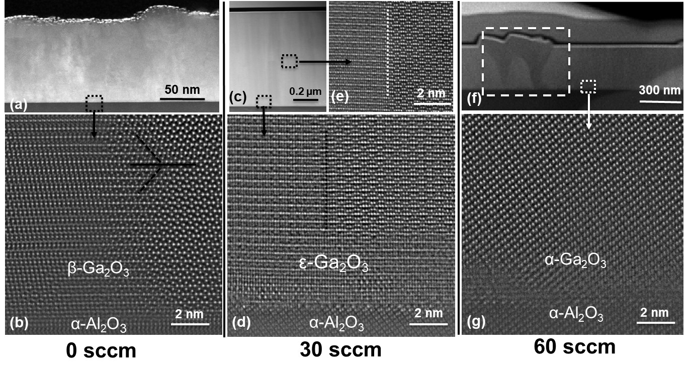
It was predicted that the HCl flux can tune the relative energy between different phases of Ga2O3 films and the predictions are consistent with their experimental observation. Essentially, the most stable β-phase Ga2O3 transforms into the pure ε-phase Ga2O3and then the α-phase Ga2O3 after flowing 30 sccm and 60 sccm of the HCl gas in the MOCVD reactor, respectively.
Furthermore, the team also showed the microstructure and the epitaxial relationship between Ga2O3 with different phases and the c-plane sapphire substrates, as shown in the STEM images (above).
These images are of TEM samples grown under HCl flow rates of 0, 30 and 60 sccm. Images (a), (c), (f) are low-intermediate magnification. Images (b), (d), (g) are high magnification (Gaussian high-pass filtered image) collected at the interface of the three samples, respectively. Image (e) shows details at the domain boundary along the film.
Precise control of the hetero-epitaxy on a low-cost foreign substrate is often the key to successfully making semiconductor devices in volume when a large low-cost native substrate is not available.
"Our HCl-enhanced MOCVD approach paves the way to achieving highly controllable, low-cost, large scale hetero-epitaxy of Ga2O3 films with different phases for optical and power device applications", says Haiding. "Further studies regarding kinetic models may be required to unveil the whole mechanism of the crystallization process with HCl, including doping in those films."
'HCl flow-induced phase change of α-, β- and ε-Ga2O3 films grown by MOCVD' by H. Sun, et al; Crystal Growth & Design, DOI: 10.1021/acs.cgd.7b01791


