

Depositing optical coatings with a metal-lift-off evaporator
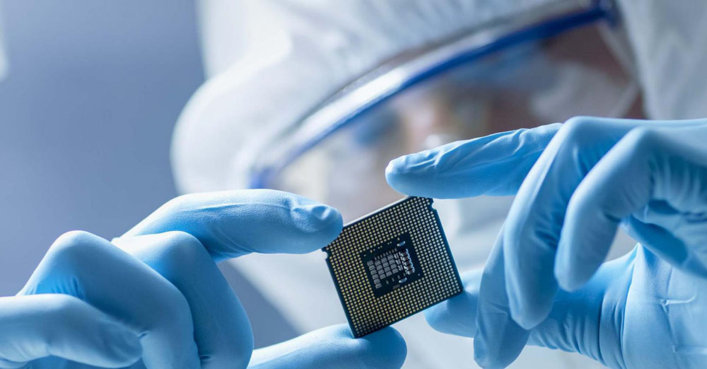
The capabilities of the Ferrotec UEFC-6100, which has a capacity of twenty-five 200 mm substrates, are not limited to efficient, uniform growth of metal layers "“ this tool can also deposit highly uniform oxide coatings by Shihu Deng and Philip Greene from Ferrotec - Temescal Division
The history of semiconductor manufacturing attests to the many advantages that come from moving to larger wafers. These benefits provide both a motivation and a driving force for the development of tools that are capable and efficient at undertaking processes on larger wafers. By succeeding in this endeavour, equipment providers can make their customers happy, by giving them an edge over their peers.
For different technologies, different diameters are adopted by the leading manufacturers. For silicon ICs, 300 mm represents the state-of-the-art. Meanwhile, for many other technologies "“ including GaN-on-silicon devices, such as microLEDs; SiC; filters, in the form of FBAR and BAW; MEMS on silicon; and thin-film batteries "“ the goal is to move to efficient processing on 200 mm wafers.
At Ferrotec of Livermore, CA, we are serving the needs of device makers with our latest generation of Ferrotec electron-beam evaporation tools. Our entire UEFC tool series is designed to deliver excellent uniformity and throughput on wafers up to 200 mm in diameter. For 200 mm wafers the UEFC-4900 can process 15 wafers/batch at a 0.9 m source-to-substrate distance, while the UEFC-5700 can process 18 wafers/batch at a distance of 1.07 m. The latest version, the UEFC-6100 further increases the batch size to 25 wafers, and can process at 1.07 m or 1.17 m for tighter design rules. This process equipment can efficiently and consistently deposit metal and oxide films.
This equipment portfolio may be better known for the creation of tools that provide efficient deposition of metals on 200 mm wafers of metals, prior to liftoff processing. However, the process equipment can also be used for the growth of optical oxide coatings.
Figure 1. The path that different regions within the wafer take through the chamber leads to a high degree of thickness and incident ion impingement uniformity.
The recently released UEFC-6100 sports these credentials, delivering excellent performance and flexibility by balancing a range of constraints, including thickness uniformity, material utilization, batch size (wafer count), and the basic metric of throughput per squarefoot of cleanroom floor space. Key features of the tool are: the conic product chamber; its capability to use two, three or four high-vacuum pumps; a dual-axis high uniformity lift-off apparatus (HULA) wafer motion, driven by non-contact magnetic gearing; a throw distance that is compatible with design rules for photo-resist structures (the incident angle must be less than 5°); and a "˜load-lock' separation between the substrates and the electron-beam source.
To highlight the capability of our UEFC-6100, in the remainder of this article we will present the results associated with the deposition of thin films with our tool. Results were obtained using a source to substrate distance of 1.17 m.
For this effort, three cryo pumps were installed in four possible high vacuum pump locations, a configuration that enables the entire system to be pumped down to a pressure below 5x10⁻⁷ Torr in just 34 minutes. If the product chamber portion alone needs to reach this pressure, pumping takes just 28 minutes. Obviously, adding a fourth pump trims those times.
We equipped the UEFC-6100 for this work with a 12 kW electron-beam power supply and a STIH-270-3CK (Poptop) electron-beam source, which limits contamination between pockets. To enable the tool to provide ion-assisted deposition, it was also fitted with a Veeco Mark-II+ grid-less end-Hall ion source.
Another feature of the UEFC-6100 is that by drawing on knowledge of the shapes of evaporation vapour clouds, the dual-axis, non-contact magnetic HULA drive maximises the evaporated material collection efficiency on a full cassette of 25, 200 mm wafers. This enables a metal deposition with non-uniformity that is near 1 percent or less across a wide range of conditions.
We are keen to stress that many features that lead to enhanced performance for metal films also lend themselves to the increased performance of oxide coatings. The design of the tool is particularly well suited to the growth of high-quality optical films, including anti-reflection and high-reflection coatings.
A compelling attribute of the UEFC-6100 is that the uniformity across multiple large-diameter substrates has little sensitivity to the multiple deposition conditions. There is very little difference in nonuniformity between materials. Note also that changes in the deposition rate, gas background and even ion source settings have little influence on nonuniformity, implying that the tuning of conditions for optical properties should not involve efforts to adjust thickness distributions via the use of varying shape uniformity masks.
Figure 3. Ellipsometry determines wavelength-dependent values for the refractive-index coefficient and the extinction coefficient.
One of the strengths of our system is its dual-axis substrate motion, which improves uniformity of ion source impingement on the growing films. During film growth, the various locations on the wafer intersect with different intensity regions of the ion source (see Figure 1). The complex path taken by the wafer helps to increase the level of uniformity of the incident ion flux across the full surface.
Optimised optical coatings
To demonstrate the advantages of our tool, we deposited individual layers of SiO2, Ta2O5 and TiO2, as well as optical coatings formed by stacking these oxides. Of great promise is TiO2: it has a very high index of refraction, giving it the potential to improve the performance of many optical designs. For example, in a quarter-wave high-reflectance stack, the tremendous contrast in indices between this oxide and a far lower index material increases the peak reflectance value and the width of the high-reflectance band. However, TiO2 is a challenging material to deposit, for reasons we shall detail in due course.
A non-uniformity range of around 1 percent, as realised in the system for pure metal depositions, can also be maintained with ion-assisted oxide films. This can be seen in measurements of the thickness variations in SiO2, Ta2O5 and TiO2 films that are grown on 200 mm substrates (see Figure 2).
To evaluate the quality of these films, we employ spectroscopic ellipsometry to determine indices of refraction and extinction coefficients. The values obtained reveal that all three materials exhibit very low absorption in the visible and the near-infrared range (see Figure 3).
Figure 4. Reflectance values, obtained at 24 positions over a 200 mm glass substrate with an eight-layer stack of SiO2 and Ta2O5.
Spectroscopic ellipsometry can highlight a significant weakness associated with TiO2: its index of refraction is more sensitive to deposition conditions than that of other oxides. The index of refraction is influenced by both the uniformity of the deposition rate and the ion flux incident on the growing film. However, the good news is that with the UEFC-6100, films of TiO2 have very uniform thickness and film properties across the entire 200 mm wafer, thanks to the complex movement of substrates through high and low flux regions. Across the full substrate area, the average index of refraction at 550 nm is 2.44, and the "˜onesigma' variation is only 0.16 percent.
These results are encouraging, but what is critical is the capability for multi-layer stacks. To investigate this, we began by growing quarter-wave stacks. They are common building blocks for high-reflectivity coatings, such as distributed Bragg reflectors.
Table 1. Variations in reflectance profiles, judged in terms of "˜one-sigma' values', highlight the high degree of uniformity possible with the UEFC-6100.
One of the structures that we have grown is an eight-layer, quarter-wave stack of SiO2 and Ta2O5. Measurements at 24 locations highlight the high level of reflectance uniformity across this 200 mm wafer (see Figure 4 and Table 1).
We have also produced a 16-layer, quarter-wave stack of SiO2 and Ta2O5. Its reflectance profile has a very high degree of correlation with that of a model (see Figure 5), with the results showcasing the potential of this stack as a building block for coatings such as a DBR.
In short, our efforts show that although the UEFC-6100 has been initially designed for metal coating uniformity and efficiency, it capabilities have much promise for the production of optical coatings.
Figure 5. There is a high degree of correlation between the measured values of reflectance for the 16-layer quarter-wave stack of SiO2 and Ta2O5, and the result generated by the model.


