

Mastering MOCVD of GaN HEMTs
There is no doubt that GaN is a great material for making electronic devices. It enables high power densities, great efficiencies and elevated operating temperatures; it sports high levels of mechanical stability, hardness, and thermal conductivity; and it has a very low sensitivity to ionising radiation. Armed with these attributes, GaN devices are unlocking the door to a new generation of commercial products that are far smaller, lighter and less power hungry than their predecessors.
One sector where these devices are making an impact is power electronics. Here, concerns relating to integration and reliability are getting retired, and sales are on the up, thanks to the superior performance and smaller form factors offered by GaN over the incumbent technology, silicon. Revenue is tipped to rocket over the next few years, according to many market research firms including Yole Développement in its Power GaN report, 2017 edition (see chart). Primary drivers include growing sales of devices that operate at around 200 V and are used for the likes of wireless charging, LiDAR and class D amplification, alongside those at around 600 V to 700 V that are used in power supplies in data centres and electric and hybrid electric vehicles.
The other significant sector for GaN electronics is RF. The impending roll-out of 5G is great news for the makers of these devices, which are already being used in base stations, and could extend their reach into micro and metro cells and potentially on to femto-cell/home routers and eventually handsets.
Veeco's Propel MOCVD System provides excellent withinwafer uniformity on 6-inch (left) and 8-inch (right) wafers in terms of (from top to bottom) thickness, composition, and bow control.
Helping to drive down production costs is the method of operation for the Propel tool: it is held in vacuum throughout the production campaign. This eliminates the need to open the chamber, and aids the use of longer production campaigns “they can exceed 120 runs. Operating in this manner, uptime can be more than 90 percent.
One of the reasons that production costs are so low is that the growth rates with the Propel System are up to double those for batch tools. The higher growth rate, realised without compromising crystal quality and reducing the total cost per wafer, is due to the high dynamic range of the V/III ratio injected across the substrate.
Great performance goes hand-in-hand with very competitive production costs. Using the Propel System, our engineers have demonstrated epitaxial stacks for RF and power devices that meet performance targets at the lowest competitive overall cost, in the context of both development and production environments.
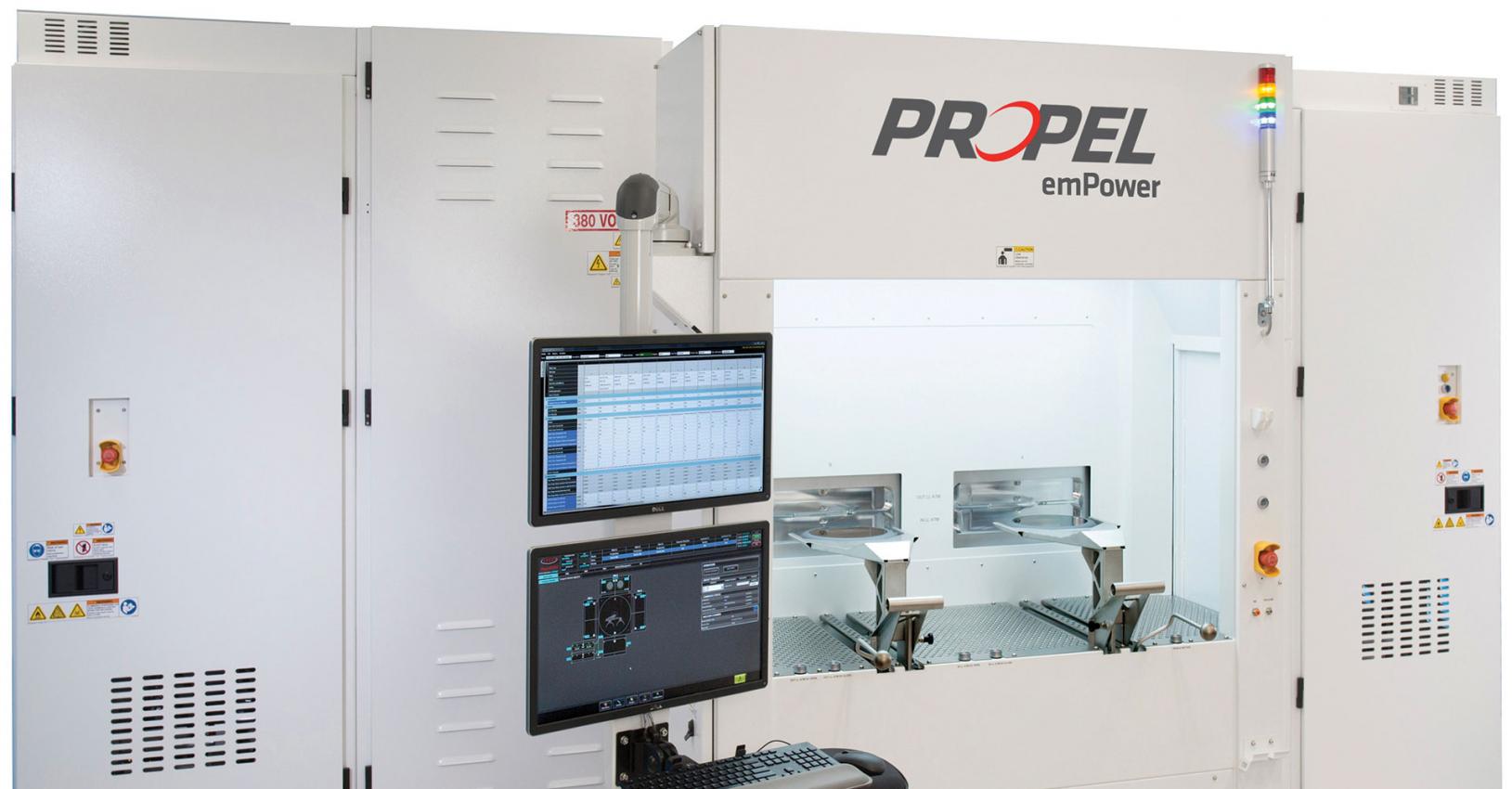
At Veeco Instruments we are addressing all these needs of the makers of GaN-on-silicon HEMTs with our Propel MOCVD System. This single-wafer tool may raise a few eyebrows, given the historical usage of batch tools in the compound semiconductor industry. However, our approach follows in the footsteps of those taken in the silicon semiconductor industry, which has switched from batch silicon epitaxy tools to single-wafer successors to realise best-in-class performance.
A single-wafer solution
That's not to say the GaN HEMT is perfect. Production of this device - including costs for epitaxy and downstream device processing and packaging - is higher than that for the silicon MOSFET. What's more, performance is hampered by charge trapping and current collapse, issues that are being actively resolved to fulfil reliability targets.
In both the power electronics and the RF sectors, the dominant GaN device is the HEMT. This device, which can be grown on a SiC substrate but is increasingly on silicon, is vastly superior to the silicon MOSFET, thanks to a breakdown field that is higher by an order of magnitude, a higher electron mobility, and a higher power efficiency at high frequencies. These strengths enable the GaN HEMT to produce a high current density and fast switching with a low drain-source resistance "“ and to ultimately lead to a smaller footprint device with high-temperature operation and low conduction and switching losses.
The sharp interface enabled by a single-wafer Propel MOCVD System provides a high two-dimensional electron gas mobility. Higher mobility in turn enables higher threshold voltage and frequency response with lower on-resistance and current leakage, enhancing device reliability.
To trim running costs even further, we have designed the Propel System so that minimal parts are required for operation. Our users benefit from the lowest consumables cost compared with other MOCVD systems, thanks to improved wafer carriers and particle filters. With our single-wafer system, the injector remains clean at all times, making it ideally suited to both R&D and production.
We know that when our customers are developing new products, they need MOCVD tools that have wide process windows, so that they can explore the entire process space; and faster learning cycles with reduced numbers of processed wafers. Most current batch systems fail to do so. That's a major impediment, because it severely limits the development and hampers further optimization of GaN HEMTs for power and RF applications.
Within the silicon industry, single-wafer tools are used in a multiple chamber configuration. So that our customers can enjoy the same benefits, we have designed the Propel System to be used within our multiple chamber system, to provide the highest yield and uptime.
Market analyst Yole Développement is predicting that the GaN device market will rocket over the next few years
For success in the market place, it is essential to combine low production costs for the GaN HEMT with high performance. So it is critical that the epilayers of the chip are high in quality and have excellent uniformity and run-to-run stability, to ensure production of consistent products with a high yield. The Propel System helps engineers to excel in this endeavour.
Propel's pedigree
Part of the reason behind the success of the Propel System is that it draws on established, high-performance technology developed over many years. For example, Veeco's TurboDisc technology provides best-in-class composition uniformity for the AlGaN and InAlN barrier layers. And within-wafer uniformity is designed into the tool, by leveraging complete elimination of residual carrier effects, combined with our proprietary Uniform FlowFlange and SimmHeat technology. Additional key features are seamlessly integrated bow measurements, direct on-wafer temperature control and the siting of the pre-cursor injector zone away from the boundary layer "“ together, these features help to ensure run-to-run stability for a wide range of process conditions.
Uniformity of the doping is also far better with the Propel System. Thanks to uniform injection, uniform carbon doping can be realised consistently from the centre of the wafer to its edge. That's not the case for cross-flow-based systems producing linear depletion. With smaller substrates, complex impertinent layers can be added to tackle this issue. However, that's not so easy with larger substrates.
Veeco’s Propel MOCVD System provides predictable outcomes for GaN applications in both development and production environments.
This doping uniformity results in sharp interfaces, which is further aided by the use of uniform injection across the substrate, and very low residency times. In contrast, planetary systems employ linear depletion, and have residency times that are up to ten times longer, leading to inferior interfaces.
Uniform injection and very low residency times also help to ensure no memory effects. This freedom equips the engineer with the opportunity to incorporate dopants such as magnesium and iron, and to optimize doping levels across multiple runs. It is a feature that is highly valued for both R&D and high-volume production.
In comparison, to eliminate memory effects in systems that inject pre-cursors into the boundary layer, such as showerhead and cross-flow reactors, engineers have to determine and optimize both in-situ baking and conditioning requirements for each stack. This severely limits R&D teams in their process window optimization.
Another asset of the Propel System is that it frees engineers from undertaking run-to-run particle management. No longer is there a need to develop and maintain chemical cleaning steps between epistack growths. Instead, inherent low particle adders are in place, ensuring best-in-class device yields.
Future proofing
Customers want to be able to use our tools for many years. To enable this, we have future-proofed the Propel System. Today, GaN transistors tend to be grown on 6-inch silicon, and over the coming years 8-inch wafers will become more common. The Propel platform configuration accommodates both sizes, and has the head room to go to even larger wafers.
Migrating to larger wafers is a challenge with some batch reactors. Due to their cross-flow design, depletion across the wafer surface restricts scaling to 8-inch wafers. But with the Propel platform, 8-inch wafers can be produced with the same uniformity and bow control as 6-inch wafers. This capability gives the engineers working with 8-inch wafers a highly versatile knob for reducing device costs. Not only are epi costs lower for 8-inch; chipmakers can generate additional savings in downstream processing and packaging costs.
Given its capability on many fronts, the Propel System is undoubtedly the ideal tool for supporting the ramp in production of GaN-on-silicon HEMTs for RF and power applications. Its merits include a very wide process window; ground breaking throughput; the lowest cost of ownership; and thanks to single-wafer TurboDisc technology, industry-leading dopant control and compositional uniformity.
Armed with these attributes, leading device companies and research institutes that we collaborate with are able to tackle the tough challenges of maximising transistor performance, trimming RF loss and harmonic distortion, and improving device reliability. Using the Propel System, these engineers are equipped with superior film-deposition control for buffer quality improvement, and are able to incorporate hard-to-deposit materials, such as magnesium and iron. More importantly, these engineers can fulfil their goal of creating a highly repeatable manufacturing process that achieves high final device yields - a feat that cannot be accomplished with such success with a batch system.


