

From LED maker to CS foundry
Q: Sanan Optoelectronics is the biggest LED chipmaker in China, with more than half of the domestic market. What is behind the launch of the foundry, Sanan Integrated Circuit, which started in 2014?
A: We want to leverage our leadership and years of high-volume, high-scale GaAs and GaN [LED] epiwafer manufacturing knowledge and expertise. We see RF, power electronics, optical and filters equally as high-volume as LEDs.
We have a large pool of MOCVD reactors from the Sanan Optoelectronics parent company's LED-chip business. From there we want to expand and explore other high-volume, high-spec lateral markets, such as RF devices for 5G cellular, IoT, Wi-Fi, 5G sub-6 GHz, power electronics - that is the high-current, high-voltage FETs and diodes used in data centres and wireless charging - and also optical. Optical includes photodiodes and VCSELs.
Q: What types of foundry services are you offering?
A: We are a process technology platform provider of compound semiconductor foundry services and are open to various types of contract manufacturing and business models, from epiwafer, fabrication, processing and DC chip probe to full-up RF known-good-die test services. We're open to any of these contract manufacturing sub-services including processing of consigned epiwafers. In RF, we carry GaAs HBTs, pHEMTs, BiHEMTs, integrated passive devices and well as SAW/TC-SAW filters. We will also offer InP HBTs. For power electronics, we have GaN-on-silicon, and SiC-on-SiC. For optical, we carry GaAs and InP for the photodiodes, VCSELs and edge-emitting laser diodes.
Q: Are you working with large companies, small start-ups, or both?
A: We service both. It's our intent and our mission to serve and focus on high-volume applications in the areas of RF, power electronics and optical. So we naturally reach, engage and seek out these fabless semiconductor companies and integrated device manufacturers who focus on these high volumes. But we are also quite aware of the upcoming and merging start-ups that serve such markets.
Q: Do you have a minimum order size?
A: For mass production, our 6-inch wafer offering comes in 18 wafers per lot. We require a one-lot minimum and a lot multiple. For R&D engineering we can support any low-volume quantity up to the point of production.
Q: How much of your business is overseas?
A: We initiated our sales and go-to-market strategy in mainland China, as our fab and headquarters is in China. But starting this year we have expanded our sales and marketing efforts beyond China to the rest of the world.
Q: How do you protect the IP of your customers?
A: To ensure and gain confidence of our customers, and the confidentiality of our GDS2 design database, we have been ISO 27001 certified. So we have strict compliance to IP and database security management control, and procedural systems for the customer's hardware, old wafers and samples, their software, and their GDS design databases.
Q: Your manufacturing capability is on a 6-inch line. Do you see that as an advantage?
A: Historically, compound semiconductor manufacturing has been on 2-inch and 4-inch. 6-inch is not new, but it's more recent. 6-inch capability, with backward compatibility to a 4-inch line, is what we offer. That benefits high-volume production. It's quick to ramp up.
Q: When a customer works with you, how long does it take from placing an order to receiving the first product?
A: Once the GDS2 is uploaded in job view, it takes five-to-seven days to produce the mask, depending on the mask layers. Then we initiate the wafer start with the mask set on. Typically, from wafer start to wafer out could go as soon as two weeks - what we call a super-hot lot. Our customers are loving their R&D engineering efforts running on a few weeks' turnaround for engineering wafers.
This is a key selling point compared with an external foundry. For GaAs, other foundries might have a couple of weeks longer lead time. But in the context of our GaAs pHEMT competing with silicon-on-insulator for switches and low-noise amplifiers, that world is more a 20-week standard lead time. Maybe a super-hot lot is 14-16 weeks at best.
Sanan IC wafer fabrication engineers processing compound semiconductor wafers.
Q: You ship full wafers and diced wafers on blue tape. Do you have partners that can provide a packaging service?
A: We don't have a specific partner to recommend to our customers. Most of the back-end suppliers for packaging and test are in domestic China, or surrounding countries like Malaysia, Taiwan and South Korea. So logistically, it helps to be shipping from our Xiamen fab to the local region for the back-end suppliers.
In the context of packaging and test, we do have a roadmap in support of copper pillar. That's coming out in Q2, to be able to support those platforms and wafers that need chip-scale package type die.
Q: Are your engineers able to offer expertise, in terms of device design?
A: We do not have in-house capability for device design. We are strictly a foundry service. Device design is more product orientated.
We do outsource and contract out limited bare-bones devices for the purposes of sampling for customer evaluation. For example, when we get customer interest in high-output- power power amplifiers, they typically want to go beyond the standard unit cell samples. They want to see some power cell samples - where these are high outputting power amplifiers - to check power handling and output power capability. So we do outsource the development, for sampling purposes, of power cells.
Q: What characterisation is undertaken for the final product?
A: When we ship die, we have DC probe test results, and we quantify the yield per wafer. We can share and review our test limits and test criteria with our end customers, which will correlate to our final test data of our products.
Q: Do you test every die?
A: We do 100 percent of the product die on a given wafer for DC chip probe. If the chip probe yield is high, the test percentage can be reduced or skipped, like for HBT products to minimise test time and therefore cost. We do have RF testing capability at the die level, but there is a cost that would be incurred for that.
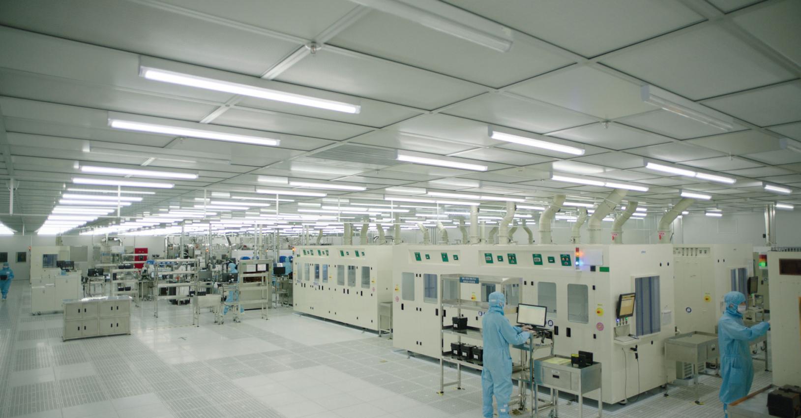
The headquarters of Sanan Integrated Circuit (Sanan IC) features China's first 6-inch GaAs wafer fab.
Q: What are your capabilities for failure analysis?
A: We have quite an extensive failure analysis lab that benefits from learned knowhow and experience from our parent company. Our lab is equipped with multiple machines, including focused ion beam; we also support transmission and scanning electron microscopy. We have a polisher, a chemical decapsulation machine, a laser decapsulation machine and emission microscopy.
Q: Tell me a little bit about the strengths of your HBT technology?
A: Sanan IC provides competitive HBT process technologies with dry etch and ledge with 0.5 micron for high power gain, compared to the conventional process with wet ledge with 1.0 micron. We also provide devices with both high linearity power and high ruggedness VSWR through epi structure design.
These performance benefits can be used for applications such as Wi-Fi 11ac/ax and 4G/5G sub-6 gigahertz power amplifiers. We are also developing InP HBT, complemented by 0.15/0.1 micron pHEMT for future 5G millimetre-
wave power amplifier applications.
Q: What is your product portfolio for power devices?
A: We offer GaN-on-silicon and SiC epi on SiC.
For GaN-on-silicon, we offer a 650 volt power GaN E-mode FET primarily intended for high power density and high efficiency AC-to-DC and DC-to-DC converters in fast charging portable chargers/adapters and electric vehicles, followed by low voltage versions - 200 volt, 100 volt and 60 volt - for more consumer-orientated AC-to-DC and point-of-load DC-to-DC power supplies such as wireless charging and backplane switch-mode power supplies for data centres and base stations. Under development is an E/D mode MISFET with two flavours: 650 volt and 1.2 kilovolt.
On the SiC side we offer different voltage and current ratings for Schottky barrier diodes. These devices could work hand-in-hand with high-power silicon IGBTs, silicon super-junction MOSFETs or SiC MOSFETs. The SiC Schottky barrier diodes come in flavours of 650 volt and 1.2 kilovolt. They range from 2 amps to 40 amps on the 650 volt. For 1.2 kilovolt, we have 10 amp and 20 amp versions. Again, these are primarily targeted to similar applications, ranging from PV inverters, electric-vehicle charging, industrial motor drivers, power factor correction and so on.
Beyond SiC Schottky barrier diodes we have a roadmap to support MOSFETs next year. We are looking at 900 volt and 1.2 kilovolt, to fill out our portfolio of high-voltage switches.
Q: What is your line-up for optical products? And how will this expand in the coming years?
A: Today, for optical we have a hybrid model. We have a traditional foundry, but at the same time our optical device division offers optical devices such as photodiodes, edge-emitting laser diodes and VCSELs.
For more advanced products, we plan to also offer electro-modulated lasers and tunable lasers in the future. For VCSELs, it will be other flavours - not just for consumers who need sensing, but for industrial applications. We also have plans for high-power lasers for medical and industrial [applications]. Our path to expand further is to commit to technology breakthroughs and innovation through collaborating with universities and the optical industry, where we'll have strategic initiatives and alliances.
Q: What are the goals for the foundry for the rest of this year and beyond?
A: Our goal for the rest of the year is to expand our customer engagement beyond China, into APAC, North America and Europe. We've started doing that for the last few months.
Our goal and vision is to support high-growth markets such as 5G, cellular, IoT, data centre and electric vehicle. We will continue to track those markets and react to their technical requirements and capacity requirements.
Equally important for us as we ramp up is to get worldwide market acceptance. This means good quality process technologies; good, stable, high production capability; high quality control and reliability.

Sanan IC factory in Xiamen City, Fujian, China; the country's first 6-inch compound semiconductor wafer foundry.


