

Obliterating dynamic on-resistance degradation
Vertical GaN-on-GaN power devices enable current-collapse-free performance
BY SHU YANG AND SHAOWEN HAN FROM ZHEJIANG UNIVERSITY
GaN is destined to revolutionise the power electronics industry. Devices that are made from this material can operate at high frequencies while offering low conduction and switching losses – attributes that allow the production of electrical units that combine enhanced energy efficiency with increased power density and a reduction in the size and weight of the system. It is these strengths that enable a hike in the performance of smartphone and laptop chargers, photovoltaic inverters, power supplies for data centres, on-board chargers and charging stations for electric vehicles and hybrids.
The most common form of this class of device is the GaN-on-silicon transistor. It has come on in leaps and bounds over the last decade, and is now driving the commercialisation of this technology.
One of the merits of GaN-on-silicon is the low cost of 150 mm and 200 mm silicon substrates.
But that’s not the only reason behind low-cost production: the epiwafers can be processed in fully-depreciated 150 mm and 200 mm silicon fabrication lines.
These GaN-on-silicon devices, however, are usually confronted with a challenge that could cause excess power loss, known as either dynamic on-resistance degradation or current collapse.
Recently, our team at Zhejiang University in China has shown that it is possible to overcome this issue by turning to GaN-on-GaN devices with a vertical architecture and nitridation-based termination.
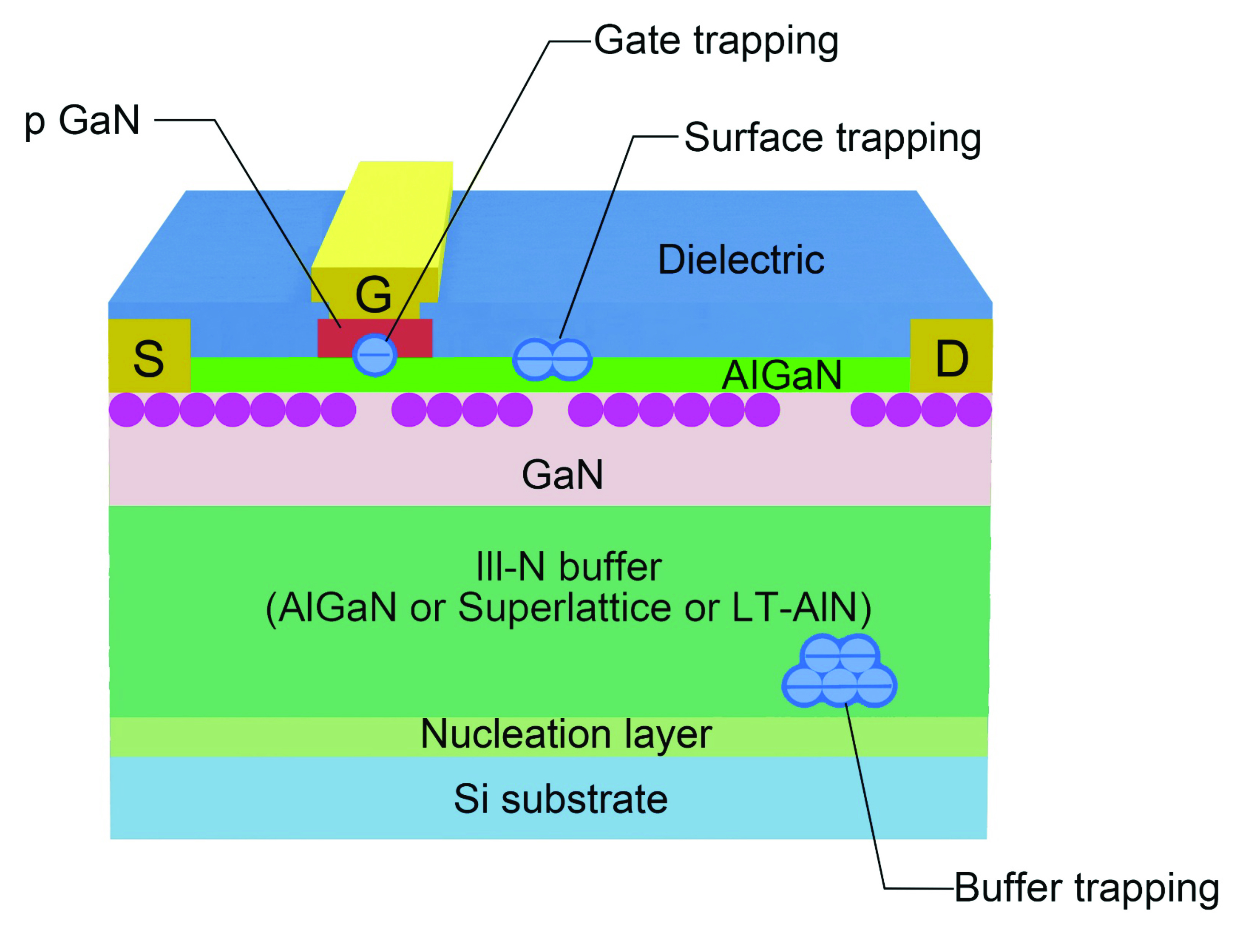
Figure 1. An illustration of trapping-induced current collapse, using a p-GaN HEMT as an example.
Trapping issues in GaN-on-siliconTo block high voltages, conventional lateral power devices comprise of a semi-insulating III-nitride buffer stack, located between the GaN channel layer and the silicon substrate. This buffer stack tends to contain a high density of bulk traps, some of which originate from crystalline defects and dislocations due to the lattice and thermal expansion coefficient mismatch between the nitride layers and silicon.
There are also deep-level acceptor traps, resulting from carbon atoms sitting on nitrogen sites. During the growth of epilayers, carbon is intentionally/unintentionally incorporated to compensate for donor-type background impurities, such as silicon and oxygen. This enables the buffer stack to exhibit a high resistivity with a low leakage.
In these lateral devices, the high-density two-dimensional electron gas, which features a high electron mobility, equips the transistor with a low static on-resistance. But when this device is switched from a high-voltage off-state, excess power loss results, due to the ailment known as either current collapse, or an increase in dynamic on-resistance.
Several factors contribute to this degradation (see Figure 1). When this lateral device is operated in its off-state with a high drain bias, the large negative gate-to-drain bias can lead to electron injection and trapping at the polarized III-nitride surface in the gate-to-drain access region. Meanwhile, in the vertical direction, the large positive drain-to-substrate voltage could cause electrons to be injected from the silicon substrate and trapped in the GaN buffer stack.
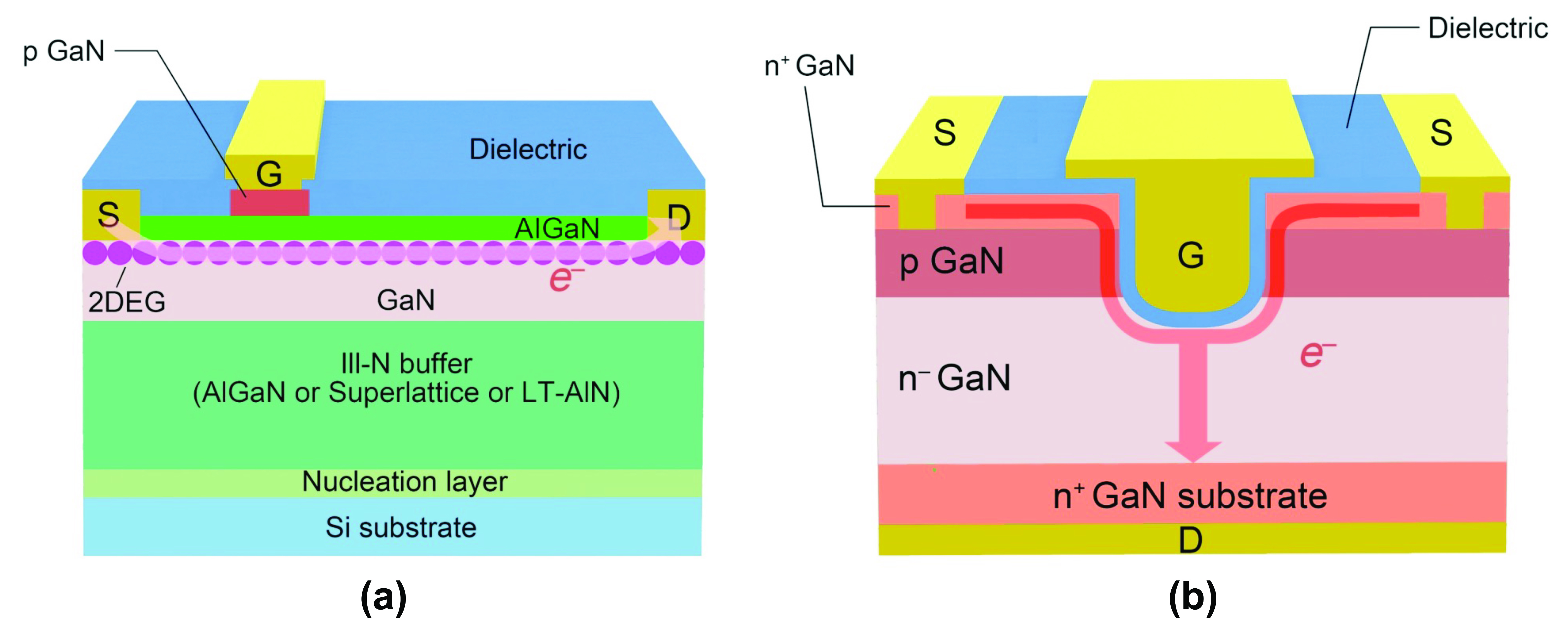
Figure 2. Schematic cross sections of (a) lateral GaN-on-silicon and (b) vertical GaN-on-GaN power devices showing different electron flows.
Another issue is that when this device is running in a high power state, a hard-switching transition can generate hot electrons in the channel. From here, these electrons may then be injected and trapped at either the III-nitride surface or the III-nitride buffer stack. When switching the device on, it may take considerable time to release electrons from surface states and buffer traps. If this happens, the two-dimensional electron gas in the gate-to-drain access region could remain partially depleted, resulting in current collapse and conduction loss.A third factor at play is that when a lateral p-GaN HEMT or insulated-gate GaN power transistor is operated in its on-state with a gate overdrive, trapping can occur in the interface and border region beneath the gate electrode. A positive shift in threshold voltage could result, creating a reduced gate overdrive at a pre-set on-state gate bias and an increase in the on-resistance.
To combat all these issues, researchers have developed multiple field plates, advanced dielectric passivation, buffer stack optimization and hybrid drain techniques for mitigating trapping effects. Despite the effectiveness of these approaches to some extent, it’s relatively difficult to completely eliminate the root cause for trapping effects, and current collapse is still regarded as one of the biggest challenges for lateral GaN-on-silicon power devices.
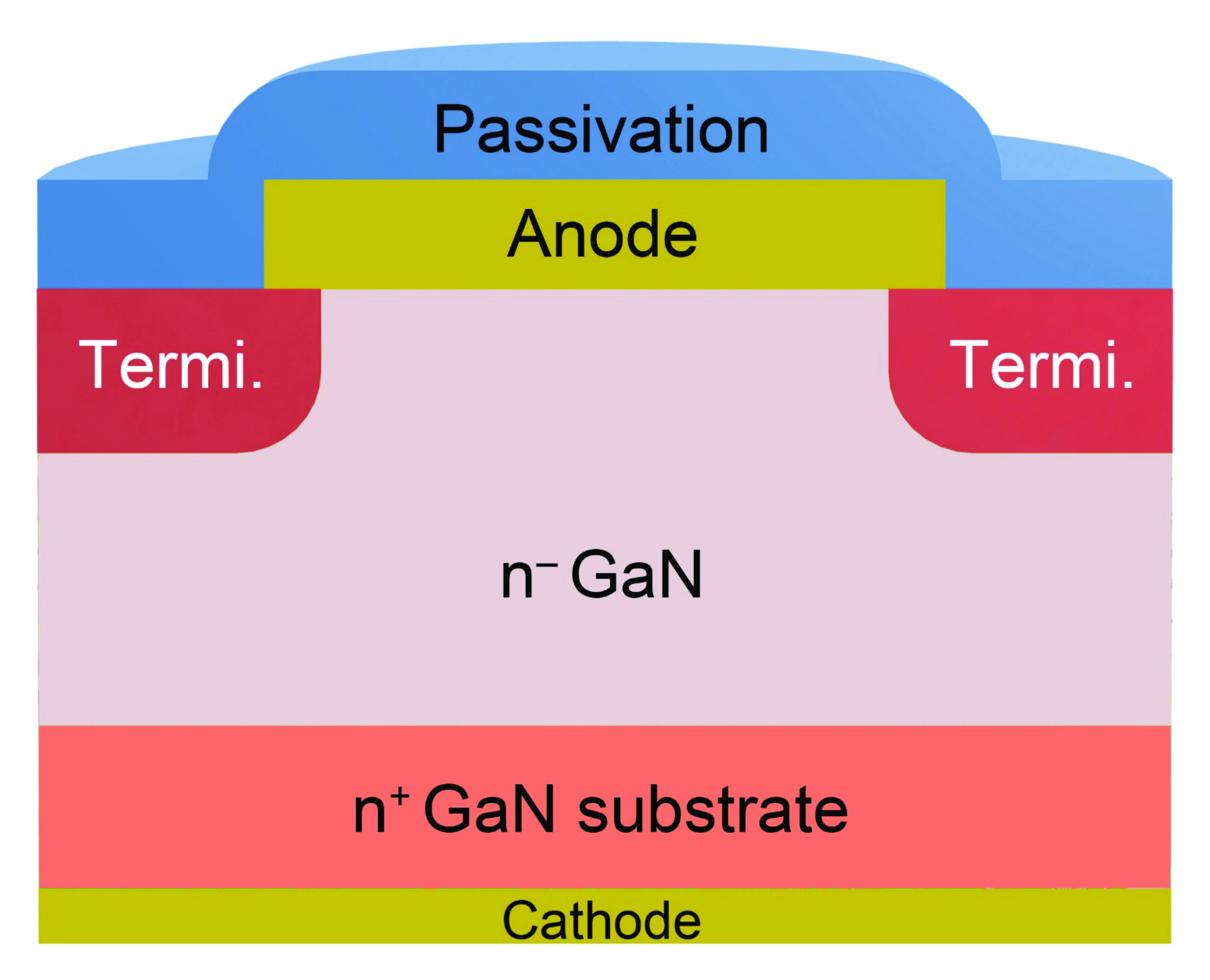
Figure 3. Researchers at Zhejiang University, China, have developed the vertical GaN-on-GaN Schottky barrier diode with nitridation-based termination.
From lateral to verticalThe recent emergence of high-quality, free-standing GaN substrates has opened the door to the development of vertical GaN-on-GaN power devices. Merits of growth on a native substrate include the elimination of lattice- and thermal-mismatch between the epitaxial layer and the substrate, making it possible to produce thicker GaN drift layers with a lower dislocation density. This architecture also trims thermal resistance, thanks to the removal of a thermal boundary resistance in the nucleation layer between the III-nitride buffer and the silicon substrate (see Figure 2). Armed with all these attributes, the vertical GaN-on-GaN power devices can deliver high current capacity, a high breakdown voltage, more efficient chip area utilization, and superior thermal performance.
A significant challenge for high-voltage vertical power devices is to address electric field crowding at the junction edge. Left unchecked, this crowding can result in excess reverse leakage and premature breakdown. The conventional approach to suppressing edge-effect-induced reverse leakage and enhancing breakdown voltage is to apply edge termination techniques. However, in GaN devices, it is not easy to implement junction-based edge termination techniques, such as junction termination extension and field-limiting rings, due to the low-efficiency of selective p-type doping and activation.
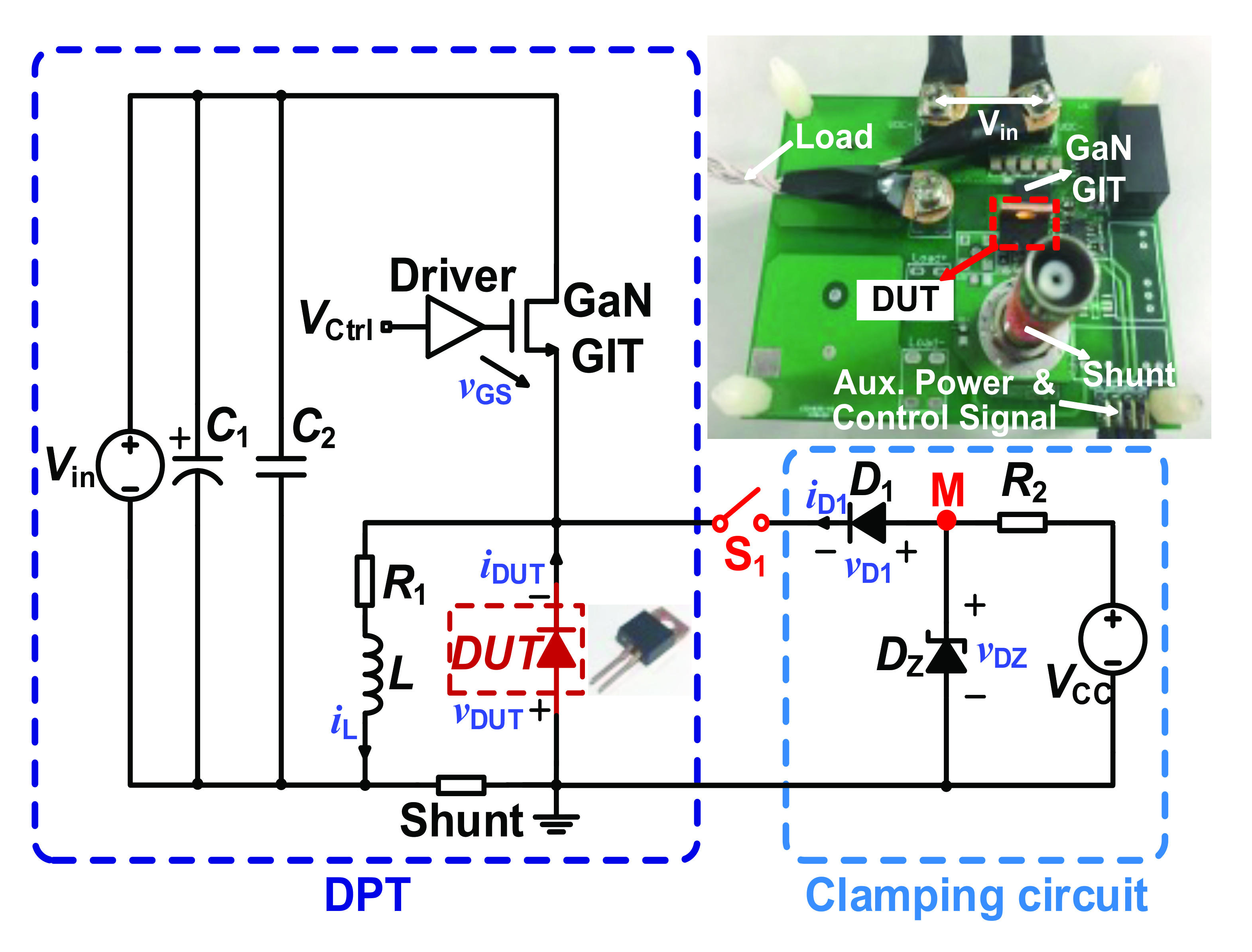
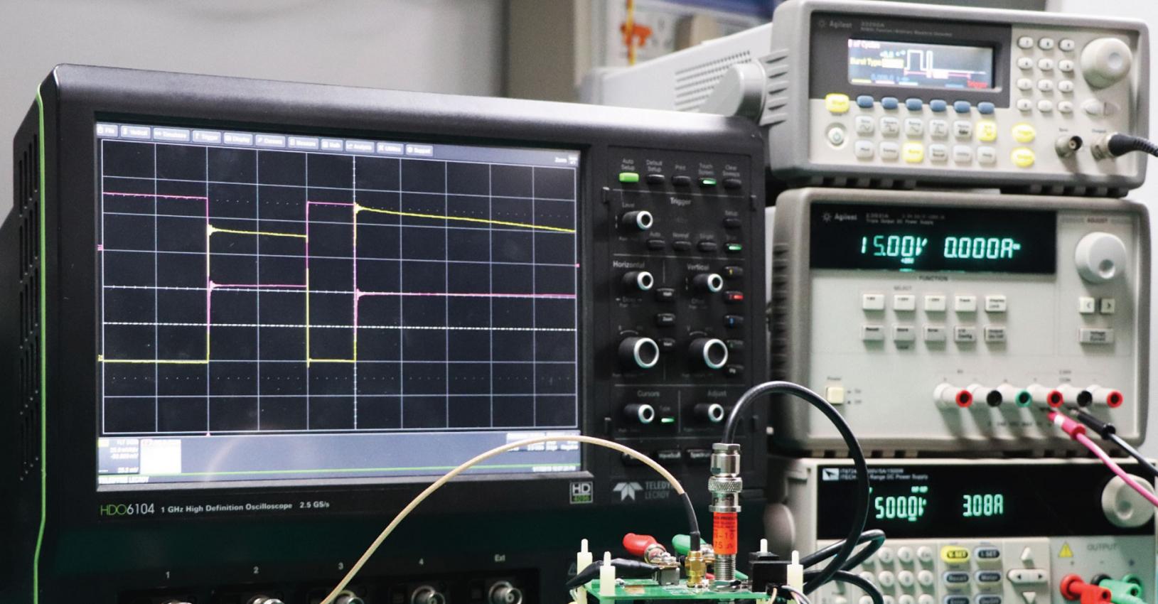
Figure 4. The team at Zhejiang University has developed a high-speed double pulse tester with a clamping circuit to provide quantitative, precise extraction of dynamic on-resistance, RON, in GaN devices.
To address this issue, we have recently developed a nitridation-based termination technique that is well suited to vertical GaN devices (see Figure 3). We form the nitridation-based termination structure by applying a low-damage nitrogen plasma treatment to the periphery of the device area with an optimal RF power and time.According to experiment, this approach shifts the Fermi-level in the nitridation-based termination region towards the valence band. This shift is most likely to result from a favourable modification of the surface conditions, such as the enhanced adsorption of nitrogen atoms and passivation of gallium dangling bonds.
One of the benefits of applying nitridation-based termination around the device periphery is that it produces an enlarged energy barrier height and/or effective barrier thickness at the junction edge. In turn, this suppresses electron transport via thermionic field emission or tunnelling, and ultimately slashes reverse leakage by four orders of magnitude while enhancing breakdown voltage – the later increases to around 1 kV. In addition to these benefits, our vertical GaN-on-GaN diode exhibits a nearly ideal Schottky contact, an on-resistance of 1.2 mΩ·cm2, and an on/off current ratio of 13 orders of magnitude.
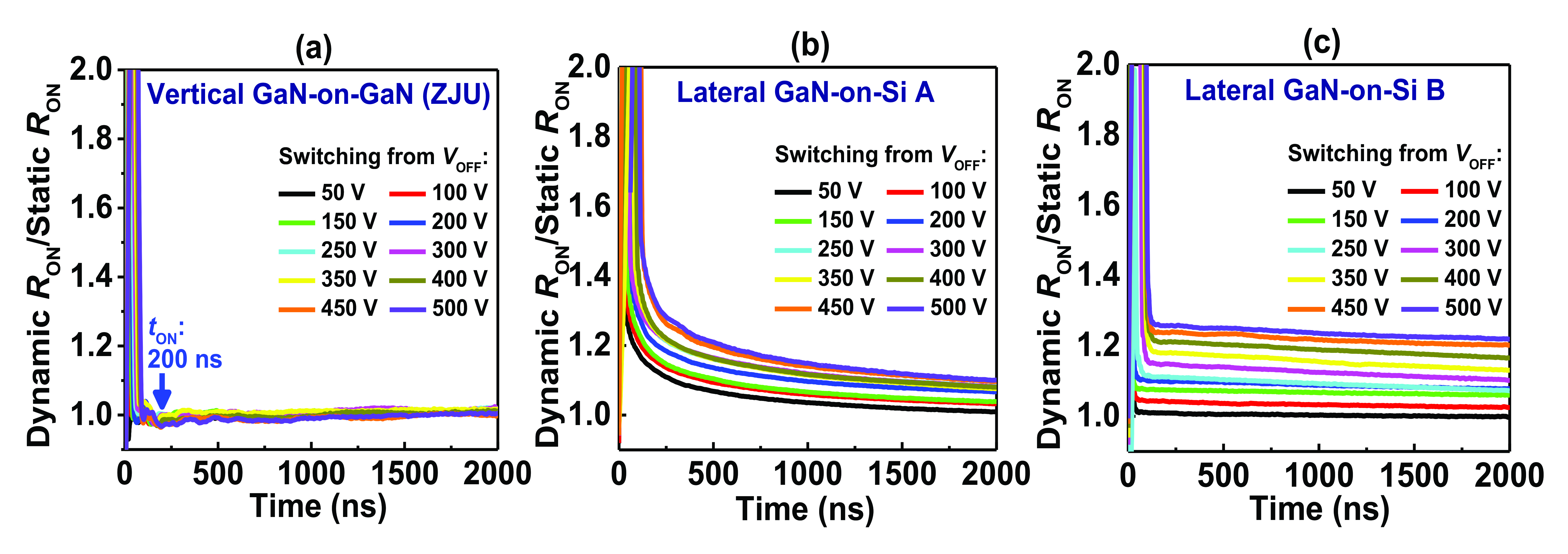
Figure 5. Time-resolved dynamic RON/static RON of: (a) a vertical GaN-on-GaN Schottky barrier diode developed by Zhejiang University; (b) a commercial lateral GaN-on-silicon device A; and (c) a commercial lateral GaN-on-silicon device B with off-state bias (VOFF) varying from 50 to 500 V.
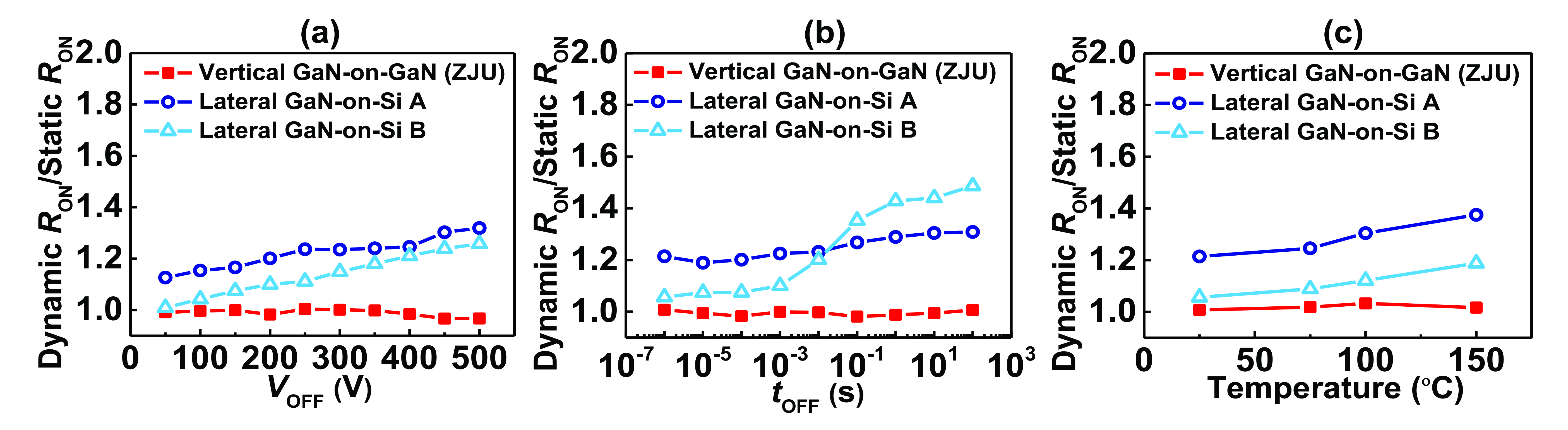
Figure 6. Dynamic RON of the three types of GaN devices extracted at only 200 ns after switching from: (a) varying off-state bias (VOFF) up to 500 V, (b) tOFF of 10-6~102 s and (c) high temperature up to 150 °C.
To evaluate the benefit of our device, we wish to compare its performance to that of a state-of-the-art lateral GaN-on-silicon device. A commercial, lateral GaN-on-silicon diode is not currently available. But we can make a comparison with state-of-the-art E-mode GaN-on-silicon transistors, by electrically shorting the gate and source terminals. With this modification – enabling the transistor to operate as a power diode when operating in the reverse conduction mode – any surface- or buffer-trapping that will impair on the conductivity of the two-dimensional electron gas leads to a change in dynamic on-resistance.Current-collapse-free performance
We have systematically and quantitatively evaluated the dynamic on-resistance under different switching conditions. Tests include: an off-state stress bias evaluation up to 500 V; an off-state stress time, over the range 10-6 s to 102 s; and elevated temperatures of up to 150 °C. The higher off-voltages and longer off-state times in the tests could impose more severe stress on devices by inducing field-enhanced electron injection and accumulated charge trapping.
All of these tests demonstrate that our vertical GaN-on-GaN power rectifier is free from dynamic on-resistance degradation just 200 ns after switching from a high-voltage off-state, outperforming the state-of-the-art lateral GaN-on-silicon devices (see Figure 5 and 6).
This result is significant – it is the first time that there has been quantitative experimental verification that vertical GaN-on-GaN devices are capable of delivering a current-collapse-free performance and overcoming the grand challenge of dynamic on-resistance.
We attribute this superior dynamic performance to several strengths of the device. Firstly, as current flow is along the vertical direction, the diodes are inherently less susceptible to surface-trapping than cousins with a lateral architecture. In addition, there is minimal bulk trapping, thanks to the high crystalline quality in the homoepitaxial epilayers and the well-controlled background/compensation doping in the drift layer; and our nitridation-based termination technique can suppress edge leakage and enhance breakdown voltage through a favourable surface modification, rather than creating deep-level traps which could adversely influence the dynamic performance.
All these merits have helped our GaN-on-GaN devices to obliterate dynamic on-resistance degradation, a breakthrough that equips them with the potential to deliver high-efficiency and high-frequency energy conversion.


