

Automotive market will drive further growth in SiC and GaN

Revenues will rocket to several billion dollars, thanks to a ramp in sales to the automotive sector
BY RICHARD STEVENSON
A great way to strengthen the case for a new technology is to highlight how much better it is than the incumbent. That’s the strategy that has been pursued by the pioneers of wide bandgap power devices. For many years, they have been demonstrating the significant energy savings resulting from more efficient power conversion, and the beneficial implications, including a trimming of electricity bills and an increase in the deliverable output from solar panels.
Right now, however, this industry has a new, even better story to tell –and one that is sure to capture the public imagination. It stars an underdog in the form of Venturi, a racing team that has a far smaller budget than many of its rivals. Off the pace for several seasons, it has been improving of late, and this March it caused an upset by netting its first win in the Formula Electric class. What’s is the secret to this success? The adoption of a new, superior technology, in the form of an all-SiC power module produced by Rohm.
Details of this winning module and the benefits that it delivers were discussed by Aly Mashaly, Director of Power Systems at Rohm Semiconductor, during a keynote presentation at this year’s CS International. At this meeting, held in Brussels on 26-27 March, Mashaly revealed that the benefits of using SiC, rather than silicon, were not confined to just delivering greater power from the battery. Instead, they extend to a 30 percent decrease in the size of the unit, as well as a reduction in its weight, which fell from 15 kg to just 9 kg. These improvements, which stem from the opportunity to use smaller passive components, are incredibly valuable – they allow the module to be placed in the ideal spot within the car, leading to better handling.
Venturi’s foray into SiC power electronics is relatively new. Back in season two (2014-2015), it employed an all-silicon module in its Formula E car. In season three, this evolved to the pairing of a silicon IGBT and a SiC diode, and from season four onwards, it has used the combination of SiC diodes and SiC MOSFETs.
Initially, Venturi’s cars were equipped with a 200kW inverter, operating at a 16kHz switching frequency. Replacing the silicon electronics with SiC enabled an increase in switching frequency to 24kHz, for an inverter producing an output of 220kW. Efficiency at the maximum power increased by more than 1.3 percent, and the maximum efficiency went up by 1.1 percent. However, these figures fail to show the true benefit of the switch to SiC. During racing, cars operate at a variety of loads – and at a partial load, the efficiency with SiC power electronics is more than 5 percent higher than it is with silicon.
The strengths of SiC will benefit not just racing cars, but all electric vehicles. Mashaly explained that for a car with a 33kWhr battery, switching to superior electronics can extend the driving distance – evaluated in terms of a reduction in battery charge from 100 percent to 10 percent – from 159 km to 177 km. Alternatively, a smaller battery can provide the same driving range. Given the high cost of the battery, this can lead to a reduction in total expenditure.

Aly Mashaly, Director of Power Systems at Rohm Semiconductor, gave a keynote presentation at CS International detailing the benefits of replacing silicon with SiC in the power module of a Formula Electric racing car.
Europe leads the wayDelegates gained further insight into the growing markets for wide bandgap power electronics, along with advances related to device design and production, in many other talks given at CS International. They included an insight into the electric and hybrid electric vehicle market by Hong Lin, Senior Analyst at Yole Développement.
Her analysis, which shows that where the substantial investment in electric and hybrid electric vehicles is coming from, will raise a few eyebrows. While Tesla is grabbing headlines, it is by no means making the biggest investment in this technology. According to Lin, Elon Musk’s firm has invested around $10 billion, while Volkswagen has devoted nearly ten times that to develop this technology. That substantial sum is helping Europe to lead the way, investing $150 billion, compared with $107 billion for Asia and just $39 billion for the US. Lin explained that sales of electric and hybrid electric vehicles will rocket over the next few years. She revealed that they hit 5.8 million last year, are tipped to climb to more than 10 million by 2020, and will exceed 25 million in 2024. Growth will occur in all forms of vehicle – mild hybrids, full hybrids, plug-in hybrids and battery-powered electric vehicles.
There are opportunities for wide bandgap power electronics in the DC-to-DC converters, the main inverter, the generator, and the on-board battery converter. According to Lin, switching from silicon to SiC devices could boost the battery voltage from 400V to 800V, and enable an increase in the driving range.
In mild hybrids, electronics convert the 12V output from the battery to 48V, which is used for the likes of air-conditioning, the brakes, and electric power steering. This task is a “perfect target for GaN”, argued Lin.
IHS Markit is expecting the SiC market to grow substantially, due to greater deployment of this wide bandgap material in electric vehicles.
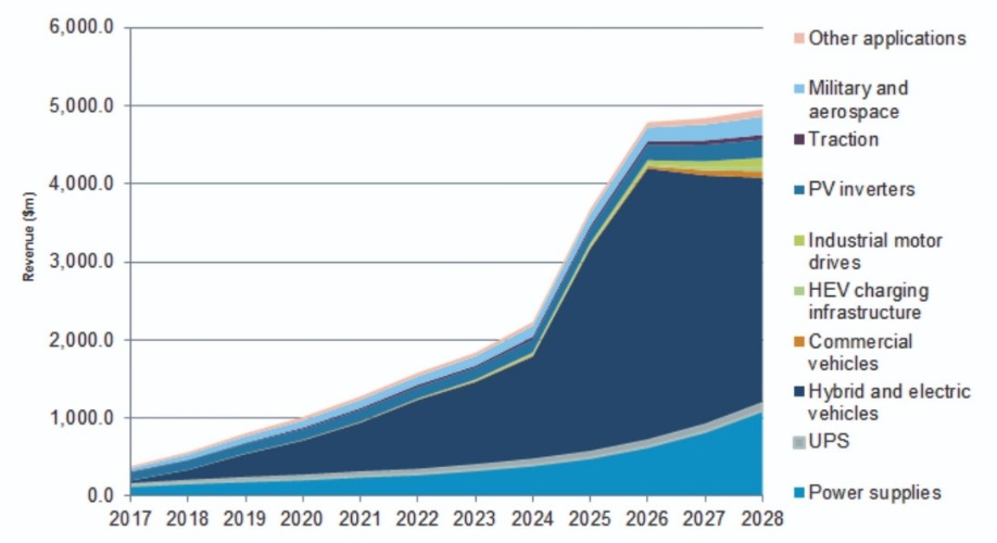
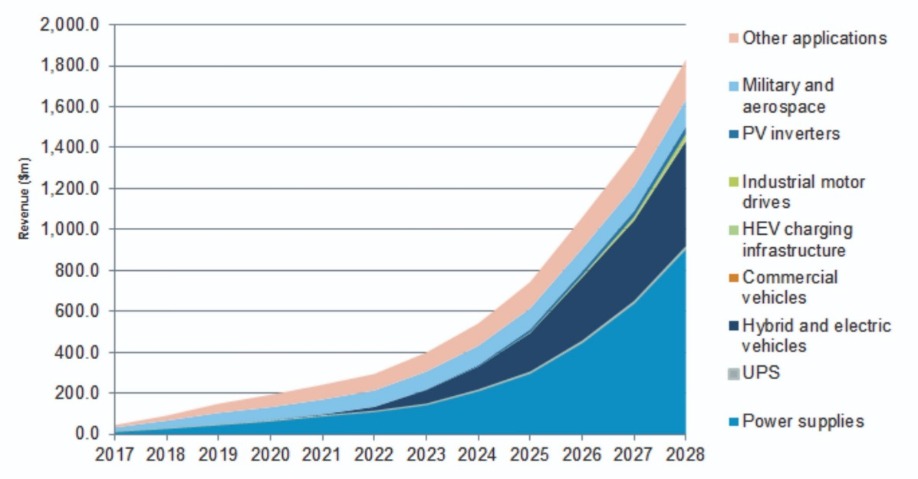
Substrate concernsA view on where all the markets for SiC and GaN power devices stand today, and what can be expected over the next few years, came from Richard Eden, a Principal Analyst at IHS Markit. Projections provided by him suggest that the global revenue for SiC totalled about $0.5 billion in 2018, will double by 2020, and then climb to almost $5 billion by 2026. In comparison, worldwide sales for GaN power devices will net around $150 million this year, and will rocket to $1.8 billion by 2028.
Two significant markets for SiC devices are photovoltatic inverters – after early success deployment of SiC fell, but it is rising again – and power-factor-correction in power suppliers. But both these sectors will be far smaller than that for electric and hybrid electric vehicles, which will take the lion’s share in the coming years.
Eden does not expect SiC to make a significant impact in either traction, industrial motor drives or wind turbines. Current handling is the issue in all these applications. “You need hundreds of amps, not tens of amps,” argued Eden.
A major concern within the SiC market is the supply of material. Although many substrate supplies have entered the market, including Dow DuPont, II-VI Advanced Materials, Norstel, Showa Denko and Sumitomo, Eden believes more are needed. Wolfspeed still dominates, with material in such high demand that Infineon Technologies and STMicroelectronics have recently negotiated supply agreements to guarantee substrate supply.
Eden noted that there has been a shift from 4-inch to 6-inch substrates, a move that was hoped to reduce costs by around 50 percent. However, this promise has not been fulfilled, due to a fall in yield.
Device results for SiC are encouraging. There are now trillions of hours of device field experience available, and data suggests that SiC diodes and transistors do not have reliability issues. What’s more, the manufacturers of these devices are meeting JEDEC and automotive AEC-Q101 standards.
Another advance is the expansion of the SiC portfolio. There are launches of SiC MOSFETs and JFETs operating at lower voltages, such as 900 V, 800 V and even 650 V. This shift enables SiC MOSFETs to go head-to-head with silicon super-junction MOSFETs with identical voltage ratings.
Dynamics in the wafer and epiwafer markets for GaN are very different from those in the SiC industry. The majority of GaN power devices are grown on silicon, so substrate supply is not an issue. Those that are making these devices can draw on the services of epiwafer providers, but that’s uncommon, says Eden. Instead, most the of production by IDMs and by foundry services involves in-house epitaxy.
The majority of GaN-on-silicon production is on 6-inch wafers, with volume ramping slowly, while 8-inch GaN-on-silicon is yet to take off. Alternative foundations for GaN are failing to make much headway, according to Eden. Although growth on bulk GaN is being aided by the reduction in the price of the substrates, due to the collapse of the laser diode market, interest in this approach has taken a knock, due to the collapse of Avogy, the premier pioneer of this technology. Meanwhile, other alternatives – sapphire, SiC and ceramic wafers, such as that made by Qromis – are known to offer performance benefits, but they are perceived to be unnecessarily expensive compared with GaN-on-silicon.
When it comes to devices, GaN transistors are now in mass production, being deployed in server and telecom power supplies, and also in power adapters and chargers. Automotive systems suppliers are also looking at this technology, which is being considered for on-board chargers and DC-DC converters.
According to IHS Markit, the global GaN device market will take off over the next decade.
Printing transistorsOne option for increasing the capability and commercial impact of GaN power technology is to unite it with silicon CMOS. At X-Fab, they have been developing processes to do just this, which were detailed in a presentation given by project manager Ralf Lerner.
Lerner argued that the benefits of GaN and CMOS integration include: reductions in interconnect distances and losses, leading to improved performance; a smaller form factor; a trimming of power consumption; and lower costs.
According to Lerner, there are two types of approach for this form of integration. One is monolithic. However, when this is performed on CMOS, the challenge is to address the incompatibilities in materials and thermal budgets; and when this is undertaken on GaN, the resulting technology is held back by being restricted to simple logic, and a lack of GaN PMOS. The alternative, heterogenous integration, can be accomplished by either direct wafer bonding, which is impaired by restrictions on chip size and wafer diameter – or by micro-transfer printing, the approach adopted by X-Fab.
Engineers at this fab start with a densely packed source wafer, and use an elastomeric stamp to transfer arrays of dispersed devices to a target wafer. Etching silicon beneath the transistor aids the removal of the devices, with a fast pick-up providing high adhesion, and a slow release producing weak adhesion that assists the printing process. On-wafer metallisation completes heterogeneous integration.
Measurements on transistors with a 17 µm gate-drain spacing, made using devices with an epitaxial thickness of just 5 µm, produce a drain current of just 1 µA at 1800 V. According to Lerner, the breakdown is primarily determined by the lateral gate-to-drain spacing, rather than the buffer thickness.
There are drawback with this printing approach. Yield depends on more factors than it would do for a conventional approach, as it is influenced by the quality of the source wafer, the target wafer, and the printing yield. There is also a trade-off between printing costs and material losses. However, this printing approach also has many merits. Lerner pointed out that: it allows for optimised processes for CMOS and GaN; it offers flexibility in chip and wafer dimensions; and it realises a low ohmic metallisation at the wafer-level, which aids heat spreading.
Boosting blocking voltages
For blocking voltages of 1 kV or more, the leading rival to silicon is SiC. But GaN can also operate in this domain, thanks to a variety of advances in GaN-on-silicon technology. These include improvements to epitaxial growth and selective removal of silicon. Both options were discussed by Farid Medjdoub in a keynote presentation.
Medjoub began his talk by championing the lateral GaN device, which is the more common architecture. He argued that its merits include the highest electron mobilities and the best cost-to-performance ratio.
The challenge to realising a higher blocking voltage, such as 1 kV or more, is the need for a thicker buffer layer, which can increase wafer bow and defect density, while compromising reliability.
Carbon-free buffers, produced by drawing on expertise at Allos Semiconductors, address all these issues. For a 6.6 µm-thick buffer featuring several interlayers, GaN-on-silicon epiwafers have a concave bow of just 23 µm, while trapping of carriers in the material is low all the way up to 1 kV. “The vertical breakdown voltage is 1400 V, which is state-of-the-art,” said Medjdoub.
He has also evaluated material from EpiGaN, which has a total thickness of just 5 µm. Using a reference buffer that has been optimised for 650 V applications, measurements on the heterostructure reveal very low trapping up to 1.2 kV. “This is another example that 1200 V is reachable with GaN-on-silicon,” argued Medjdoub.
Even higher voltages are possible with selective substrate removal. Values of 3 kV have been reached by first removing the silicon below the buffer layer, before adding a 15 µm-thick film of AlN by PVD, followed by a 2 µm-thick film of copper. Medjdoub and his co-workers are now working with
ON Semiconductor to apply this approach to industrial devices that are 4 mm-wide, normally-off, and capable of delivering a current of 10 A or more. Testing shows low trapping up to 3 kV, indicating that the silicon replacement does not induce additional trapping effects.

Hong Lin, a Senior Analyst at Yole Développement, predicts that sales of electric and hybrid electric vehicles will climb to more than 10 million by 2020 and to over 25 million in 2024. Growth, which will spur sales of SiC and GaN devices, will occur in all forms of vehicle – mild hybrids, full hybrids, plug-in hybrids and battery-powered electric vehicles.
Advantages of AI
During the production of power devices, epiwafers are inspected for quality control. It is usual to use bright field, dark field and differential interference contrast to identify and categorise defects on the surface. But what about buried imperfections?
According to Shivanui Lyer, a solutions architect at Nanotronics, these can be exposed by ultra-violet photoluminescence. In her presentation she showed a wide range of defects, exposed by ultra-violet photoluminescence with different excitation wavelengths.
Classifying defects is time-consuming and tricky, and the use of artificial intelligence promises to streamline and improve this process. Nanotronics have taken this approach, investigating the capabilities of artificial intelligence and comparing the results with those obtained with an operator. When they discovered a discrepancy, further investigation revealed human error. “We were thrilled. We had achieved super-human results,” remarked Lyer.
Superior SiC substrates
With demand for SiC substrates at a high, it is important that this industry obtains a high yield from every wafer, to ensure as many high-quality devices as possible get to market.
One way to do this, argued Revasum’s CTO, Robert Rhoades, is to use single-wafer processing, along with robotic handling. He claimed that compared to a batch approach, this enables a higher degree of precision, increased reliability, and ultimately a boost in yield. “Yield is key,” argued Rhoades. “It trumps other concerns.”
Revasum’s single-wafer tools are used to polish substrates. They employ a grinding approach, with a fixed abrasive. This is said to lead to far less sub-surface damage to the substrate than the batch-based lapping approach, which employs loose abrasive and creates more sub-surface damage. Note that the removal of material is far faster with grinding, so the throughput of the multi-wafer tool is not as significant as one might expect.
Another benefit of the single-wafer process is that during the polishing process, the slurry and debris, described by Rhoades as being like “microscopic concrete”, is less likely to adhere to the substrate. This means that with a batch approach, the slurry and debris might dry on the wafer during unloading, a situation that does not occur with single wafers, which benefit from a wet-in, wet-out process.
Getting the best out of every substrate is essential right now. Demand for SiC transistors and diodes is increasing, and must be fulfilled with high-quality products to support further growth in the market. With GaN, it’s a slightly different story.
Here, sales are smaller, but again a great future awaits. To find out just how good it will be, and get an update on the progress of all wide bandgap devices, make sure you attend next year’s CS International.


