

Embarking on epiwafer production in China
Founded just a year ago,
WaferChina is on a mission to become a substantial supplier compound
semiconductor epiwafers to the domestic market. Richard Stevenson
catches up with its CEO, Ping Gong, who outlines the growing markets for
its products, manufacturing challenges, and the company’s expansion
plans
Q: What are the long-term goals for WaferChina?
A: The long-term goal is to make WaferChina the number one VCSEL epiwafer supplier in China. China is very heavily reliant on importing epiwafers.
Q: Your company is focusing on GaAs-based optoelectronic materials, and in particular, VCSELs. Why does the world need another supplier of epiwafers for GaAs-based VCSELs?
A: Right now, there are new opportunities. People are talking about AI and 5G. These new technologies are coming to your life and my life. With these new technologies, you need a lot of semiconductor lasers and detectors. Smart cars are coming, smart phones have been on the market for years, and I believe this is almost a revolutionary time for changes in industry, in terms of the car, the phone, and homes.
For this you need a lot of semiconductor chips and wafers. In China, there are some chip companies that are growing, but there is a lack of epi-companies. The chip companies are very heavily relying on the importing of epiwafers. So there is an opportunity in China for domestic epi-wafer suppliers.
Q: What do you see as the biggest markets for the GaAs VCSEL?
A: The biggest market is for commercial electronics – for instance, the phone application. The Apple brand has brought the VCSEL into bigger market production. I see this as opening the door for applications of VCSELs in 3D applications.
Datacoms are a stable market for VCSELs, and are growing steadily, as they have been over the last decade. But I think the market will be much smaller than that for 3D applications.
Q: Who are the biggest VCSEL makers, in terms of devices? And do they tend to outsource the epi, do this in house, or a combination of both?
A: Right now, Apple’s supplier is Lumentum. Lumentum largely relies on IQE’s epiwafers. It has some R&D activity, in terms of epi, but not mass production, from what I understand.
There are some other companies, like II-VI. They have in-house epi, and they are making chips themselves. They are more integrated. Also, there is Finisar. They are pretty integrated.
There is a relatively new VCSEL player AMS. They have invested a lot in the last two or three years, in terms of VCSELs. They acquired Princeton Photonics, so a fabless company with expertise in designing. They have set up their own manufacturing in Singapore with MOCVD reactors and a chip production line with 6-inch wafers. But as far as I know, they are still in the ramping up stage in terms of epi and not in mass production yet.
Q: How big is the VCSEL epiwafer market, in terms of the number of wafers per year?
A: From my understanding, the current market is about 50,000 6-inch wafers. That many is consumed by one phone company. With Android systems coming up now, I believe that number will go up very quickly.
Q: You are based in ShaanXi Optoelectronic Incubation Centre. Is that a supportive location for your venture?
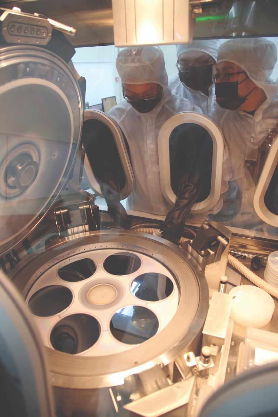
A: The biggest benefit of the incubation centre is that it helps the company to start very quickly. Our MOCVD tools moved in at the end of March and the beginning of April 2018. We started sampling from July 2018. So that was a really fast start.
The incubation centre doesn’t give any cash support, but it gives facility support. It has a cleanroom, and some equipment. Our company has only bought MOCVD reactors and some characterisation equipment.
Q: Tell me about the very early days of the company. Where did the idea come from, and how did it get off the ground?
A: The motivation for me to set up the company is the VCSEL market taking off. I have been involved in VCSEL epitaxy over the years, and the market has never been big enough. But from two years’ ago, when Apple had this face recognition application, the VCSEL became a really hot product. I realised that there are huge opportunities, so I decided to set up this company to do this business.
In China there are no volume VCSEL epi-wafer suppliers. And the market is huge. In the phone market, China is 60 percent of the world. The car industry is also very big. So there are lots of opportunities in China.
Q: How long can you stay in the incubation centre?
A: There is no time limit, but capacity is limited. The cleanroom can have up to eight-to-ten big MOCVD reactors. So before we grow any bigger than that, we can stay there. But eventually we will have our own production site.
Q: Who are the investors in the company? And do you get much support from the government?
A: We are a pure commercial company. We are a joint-venture between British and Chinese. We started with two local VC investors, and we have had another round of funding. Currently, we have four venture-capital investors.
Q: Will you need to find more investors to grow the company? Or could that come from re-investing profits?
A: After two rounds of funding we have now bought enough MOCVD tools. We will have to see what the market is going to do over the next couple of years. If we need to expand faster, we may have to raise more money. But if we have a more regular expansion, we can probably use our own cash flow. It’s not a problem to raise more money. There are many investors that are interested in investing in us.
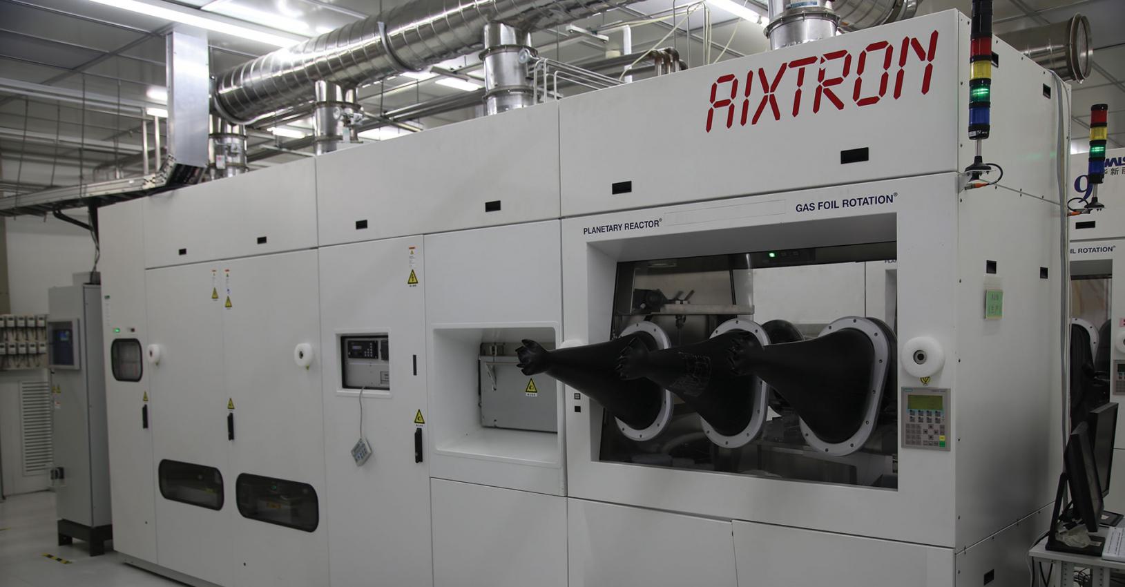
With the arrival of two more MOCVD machines in the second quarter of this year, WaferChina will have the capacity to produce more than 20,000 6-inch wafers per year.
Q: What is the headcount today, and who are the key personnel?A: We have under twenty employees right now. But we also have some engineers supporting us from the incubator centre. They provide general support, like running the facilities and gases.
I have an operations director, Qiang Zhang. He has twenty years of experience of working in silicon IC fabs. He is good with cost control and quality control. He is helping to set up the WaferChina quality system and operation
system.
Recently Andreas Eisenbach has joined our technical team. Eisenbach has 30 years’ experience in III-V compound semiconductor epitaxy, R&D, production and product management.
Q: How much capital equipment have you bought?
A: Currently, we have three MOCVD production reactors. We have ordered two more, which are coming in April 2019, which will take us up to five reactors.
The incubator centre has a lot of characterisation equipment. We have only bought some very specialised equipment.
Q: What is the capacity of your fab?
A: With the additional two reactors, we could produce more than 20,000 6-inch wafers per year. We can produce 3-inch to 6-inch epiwafers.
Q: How do you characterise your epiwafers?
A: It depends on the product. For the VCSEL we provide PL mapping, reflectance uniformity and PL wavelength data, doping characterisation and surface morphology.
For the edge-emitters, we also provide thickness data, doping data, composition data, uniformity, and PL wavelength, of course.
Q: The VCSEL is a relatively complex structure. Your company faces strong competition from the likes of IQE, that have many years of experience in making these products. How can you compete with all that experience?
A: I think that most of the IP is in the customer design. From an epitaxy material-quality point-in-view, I’m confident with our team’s more than fifity years of experience in working in the MOCVD epitaxy industry – that there are a lot of fundamental things that our team understand very well. We believe we can grow very good quality material.
Of course, a big company like IQE has its own expertise. But their major advantage, in my opinion, is mature production.
In comparison, we are more competent in terms of lead time and technical services to Chinese local customers. The flexibility of lead time and technical support is particularly important for new markets like the VCSEL. We are developing products together with our customers.
Q: Do you think it’s easier to grow VCSELs now than 20 years ago, due to improvements in MOCVD tools?
A: I would say the reactor performance has improved, but fundamentally, there is still a need for a lot of experience, especially in trouble-shooting. Let me put it this way: run-to-run uniformity is a lot better than it was twenty years ago, but from time to time there is still a shift in quality, or in uniformity. So troubleshooting, understanding the process, is still critical.
Q: Are you able to hire talented process engineers with expertise in VCSEL epiwafer growth?
A: Most of our engineers are from the LED industry. They have been trained up over the last ten months, and they are getting more competent in terms of understanding VCSEL growth. The major technology has come from our technical team’s experience.
Q: As well as a good a MOCVD reactor, high-quality metal-organics are crucial to VCSEL quality. Do you think Chinese companies are capable of producing these materials with sufficient quality, or will you be sourcing from an international supplier, such as your former employer Azko Nobel?
A: It’s not just metal-organic sources, but arsenic and phosphine. Now we can use 60 to 70 percent that is domestically produced. But there are some key materials that we are still importing, like from Azko Nobel, for critical layer growth.
Q: Are there IP issues surrounding the growth of the VCSEL? And how do they impact you?
A: I think most IP is in the epi structure design, which is with our customers. In terms of epitaxy process, I don’t think that there are too many restrictions. Basically, epitaxy is hands-on processing, and there is a lot of individual experience and trouble-shooting skills needed. Of course, we do respect IP, international law and Chinese law. The company has to be very sure we don’t run into any problems with that.
Q: Do you expect a high proportion of your sales to be domestic? Or will much of your revenue come from overseas?
A: I think the majority of sales will be domestic business, because there will be a big demand in China for VCSELs, as well as other lasers and detectors, and there is not much commercial VCSEL epiwafer supply in China. Especially with the current phone and car applications, China will be a big market, in terms of epiwafer demand. Our goal is to be world-class on the domestic market.
Of course there is no reason why we cannot sell products outside China.
Q: Does the current US-China trade war hamper international sales, but aid domestic sales?
A: I think that domestic sales may be positively impacted, because of the taxation. If you want a wafer from the US, currently you have to pay 25 percent tax. But for exporting, as far as I know, there is no tax added on. So there should not be much impact for our international sales.
The current trade war is between China and the US, and the two governments are working on a solution very actively, I believe. They will reach an agreement.
Q: Have you started to sell epiwafers?
A: Yes, we have gone through the sampling stage.
Right now we have customers buying product from us. They have gone through the qualification stage. But the volume is not big yet, because most of our customers are start-up companies, and they need to take time to qualify their customers, and develop their products.
Q: What are the goals for the rest of this year?
A: We will hopefully get into a mass production stage by late 2019, after our customers go through their qualification with their customers, the cell phone companies.
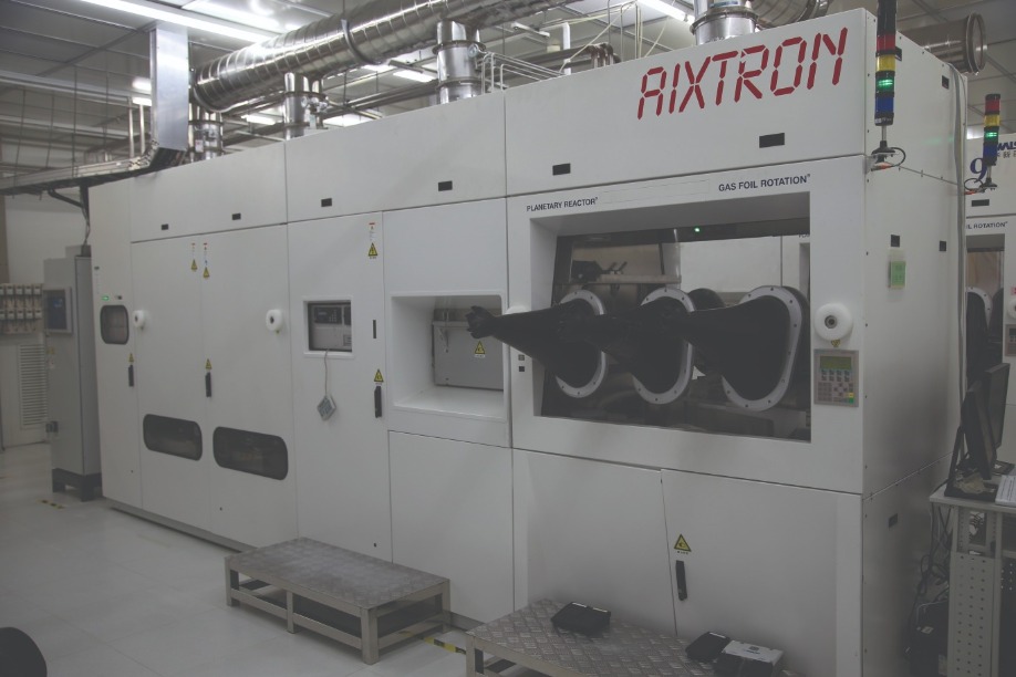
WaferChina has three MOCVD reactors for its growth of GaAs and InP epiwafers. Two more tools will be installed in the second quarter of 2019 at its facility in the ShaanXi Optoelectronic Incubation Centre.
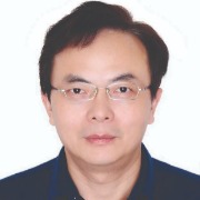
CEO and founder of WaferChina
CEO of WaferChina, Ping Gong, founded the company in April 2018. Prior to embarking on this venture, he worked for AkzoNobel for more than 12 years, initially as Marketing Manager for the Asia Pacific region, and more recently as the Global Technical Development Manager. Between 1998 and 2005 Gong held the role of Senior MOCVD Growth Engineer and then Project Manager at IQE, Cardiff. During his time at IQE, he was responsible for the production of epiwafers for various lasers, including several types of VCSEL. He holds a PhD in Optoelectronic Materials from The Chinese Academy of Sciences, and a Bachelor’s degree in Semiconductor Devices from Xidian University, China.


