
EV to show latest in heterogeneous integration in Las Vegas
Company to present on high-vacuum system which provides direct bonding of 'anything on anything' at IEEE ECTC
EV Group (EVG), a supplier of wafer bonding and lithography equipment for MEMS, nanotechnology and compound semiconductors, will be presenting on its latest developments in heterogeneous integration and wafer-level packaging at the 2019 IEEE 69th Electronic Components and Technology Conference (ECTC), to be held May 28-31 in Las Vegas.
The papers include:
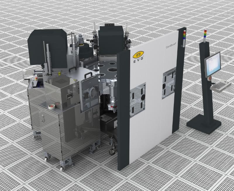
'Optimisation of a BEOL Aluminum Deposition Process Enabling Wafer Level Al-Al Thermo-Compression Bonding'. This joint paper by EVG, IHP, and Sabanci University, describes a wafer-level aluminum-aluminum (Al-Al) thermo-compression bonding process used in combination with an optimised Al sputter-deposition process. Surface treatment and subsequent bonding are both performed in a high vacuum cluster via the EVG ComBond automated high-vacuum bonding system, which provides oxide-free direct bonding of 'anything on anything'.
'Al-Al Direct Bonding with Sub-μm Alignment Accuracy for Millimeter Wave SiGe BiCMOS Wafer Level Packaging and Heterogeneous Integration' is a joint paper by EVG, IHP, and Sabanci University that examines the use of the EVG ComBond system to enable Al-Al direct bonding with high alignment accuracy and reduced process temperatures to enable low-cost, fine-pitch wafer-to-wafer interconnections supporting high-performance mm-wave SiGe BiCMOS wafer-level packaging.
'Ultra-thin QFN-Like 3D Package with 3D Integrated Passive Devices' is an interactive joint poster paper by EVG, 3DiS Technologies, Besi, and NXP Semiconductors that describes the development of a novel ultra-thin, substrate-less package that integrates ultra-thin 3D stacked dies and compact 3D inductive devices inside. The work involves the use of EVG's laser debonding solution, which combines a solid-state UV laser and proprietary beam-shaping optics to enable optimised, force-free debonding.


