

Quantitative cathodoluminescence streamlines chip production
Cathodoluminescence offers a quick, non-invasive approach to determining alloy compositions, exposing defects and uncovering surface contamination
BY CHRISTIAN MONACHON AND SYLVAIN MUCKENHIRN FROM ATTOLIGHT AND HASTI MAJIDI AND CHRIS FRANCE FROM ALTA DEVICES
All compound semiconductor chipmakers, from the producers of LEDs, lasers and solar cells to the makers of power and RF devices, need to characterize their material. It is an essential step in the production process that can expose and identify any imperfections in epiwafers, and may save money and reputation, by avoiding the production of devices with dubious characteristics.
Cathodoluminescence is one of the many techniques that may be used to characterise epiwafers. It involves directing a beam of electrons at the surface of a wafer, and collecting, in parallel, secondary electrons and an optical signature. Data extracted from these distinct signals are complementary and offer much insight into the characteristics of the material. For example, imaging cathodoluminescence intensity highlights both buried and surface defects, and the latter can be distinguished from the former using a secondary electron image taken in parallel (see Figure 1).
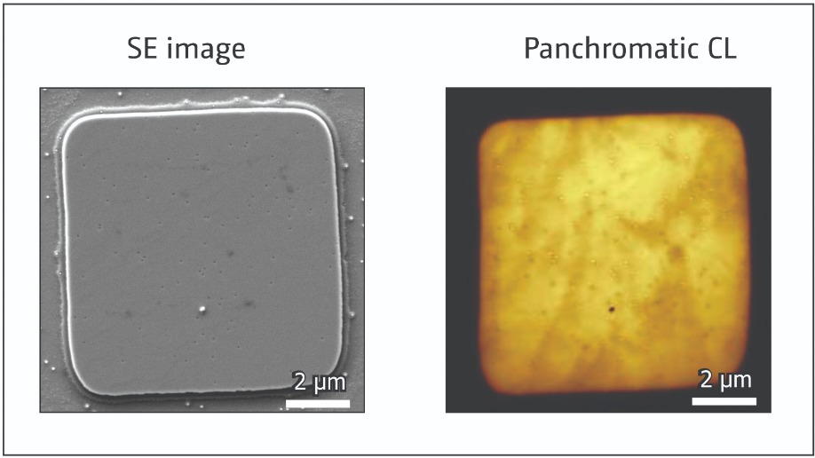
Figure 1. The Attolight Säntis 300 can provide scanning electron (SE) and panchromatic cathodoluminescence (CL) images. Shown here are 7 µm by 7 µm images of a microLED. The largest dark spot is attributed to a speck of dust, visible in the scanning electron image. Several types of buried defects can be identified in the cathodoluminescence map.
At Attolight of Lausanne, Switzerland, engineers have developed a portfolio of cathodoluminescence instruments, including Säntis 300, an instrument capable of full-wafer mapping (for details of this tool, and its capabilities, see Capabilities and strengths of Säntis 300). Read on to discover how this tool has been used by GaAs solar cell producer Alta Devices to undertake three particular tasks: to speed and trim the costs associated with developing the process for producing AlGaAs layers with well-defined compositions; to detect defects detrimental to device performance; and to expose surface contamination. Note, moreover, that Alta Devices also use cathodoluminescence for new layer design development.Characterising composition
To optimise the performance of GaAs solar cells, makers of these devices must produce homogeneous layers of AlGaAs alloys with a composition that is very close to the target value. Success in this endeavour often involves measuring the composition of AlGaAs epilayers with Auger electron spectroscopy, but cathodoluminescence offers a superior alternative.
One of the merits, benefitting the engineers at Alta Devices, is the substantial cost saving associated with preparing a reactor for its initial production of solar cells. Prior to the growth of this photovoltaic structure, calibration runs are required, with typically five cycles needed to tune homogeneity, and a further five to tune the ratio of aluminium to gallium in the AlGaAs epilayers.
Savings of around $50,000 are realised by carrying out this initial tuning with cathodoluminescence, rather than the more common approach, Auger electron spectroscopy. The reduced expenditure partly stems from making the measurement in-house, rather than shipping a sample to a specialist that will take several days to provide a result. In addition, as Auger electron spectroscopy is a destructive technique, a cost comes from being unable to re-use the base wafer.
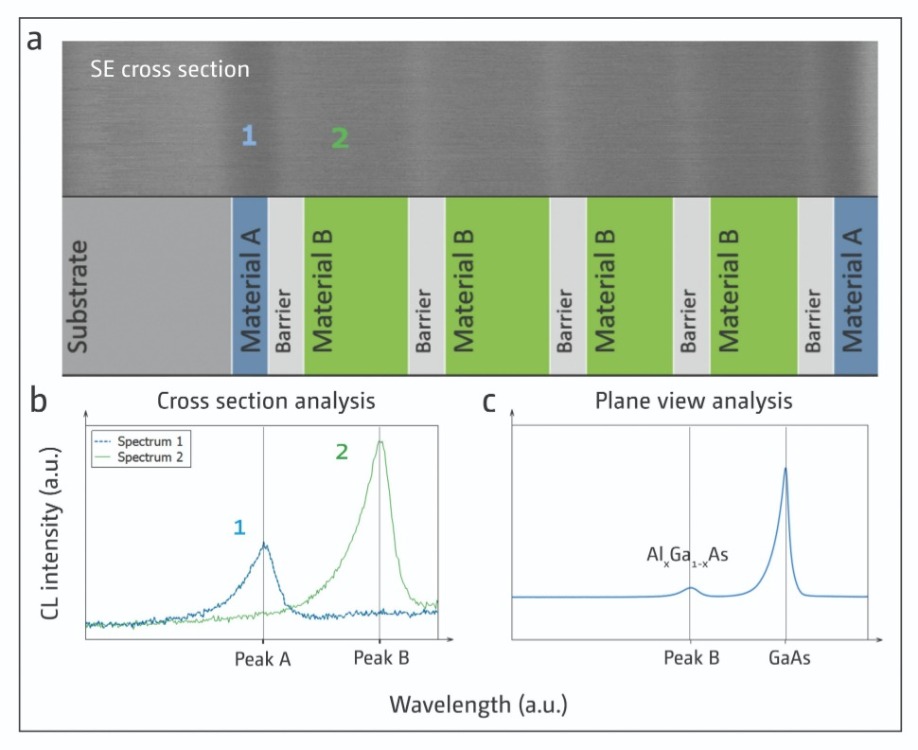
Figure 2. (top) Cross-sectional scanning-electron imaging of a multilayer AlxGa1-xAs stack together with a diagram of the structure. The sample is used for the initial cathodoluminescence calibration with respect to Auger electron spectroscopy. (bottom left) cathodoluminescence spectra extracted from material A and B, exhibiting distinct spectral features. (c) application of the obtained calibration in top view, production mode, to obtain a composition for material B.
Another advantage that cathodoluminescence has over Auger electron spectroscopy is that it offers greater insight into the characteristics of the wafer. Whether undertaking initial tuning, quality control or R&D, cathodoluminescence provides a faster turnaround and better statistics. Operating in an automated step and repeat mode, this technique can determine alloy composition at more than 120 points per wafer in less than 5 minutes. In comparison, it takes an hour to measure one point on a wafer by Auger electron spectroscopy.Cathodoluminescence is also a very powerful tool in a production environment. As it is non-contact, there is no need to scrap any base material. Instead, samples can be returned to the production batch after they have been inspected. Higher production yields are also possible – measurements typically take much less than 30 minutes, so if there is a problem with the growth process, this should become apparent before a second out-of-specification run begins.
Identifying sub-surface defects…
When producing GaAs solar cells – or, for that matter, power and RF electronic devices – a major concern is the class of defect that can cause a short circuit between the active layers. This type of defect is hard to spot, as it is not visible by either scanning electron microscopy, optical microscopy or atomic force microscopy.
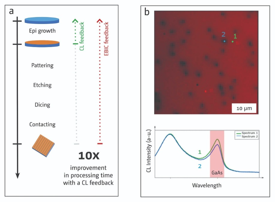
Figure 3. (left) Identifying defects with cathodoluminescence, rather than the electron beam induced current technique, trimmed the turnaround time for defect density determination and process adjustments by a factor of ten. (top right) cathodoluminescence imaging, centred on the GaAs band edge emission, exposes crystalline defects. Comparing points 1 and 2 with spectral scans (see bottom right), shows that only the GaAs peak suffers a variation. This suggests that the defect spotted at point 2 is actually in the GaAs layer of the stack, not in the other layer emitting the light in the peak to the left of it.
Prior to the availability of cathodoluminescence, defects were identified by an electron beam induced current. However, this measurement has to be carried out on the final device, resulting in a time delay before the process can be adjusted. With cathodoluminescence, this time is divided by ten, because the very same defects can be identified right after the epi process. This significantly speeds the development process and produces material with better properties – and ultimately a better average device quality. The non-contact, non-destructive nature of cathodoluminescence also pays dividends. If the material is good, production steps can proceed on analysed samples.Obviously, a non-destructive technique doesn’t save money when epiwafers are poor, and need to be scrapped. However, the speed of this technique enables a saving associated with avoiding unnecessary processing on sub-standard wafers.
Yet another merit of cathodoluminescence is the greater insight it offers, compared with the electron beam induced current technique. This aids root cause identification, because with cathodoluminescence, the layer containing the crystalline defect can be identified by its detailed spectral signature.
… and surface contamination
When surface contaminants are on the epiwafers, they tend to have a significant impact on surface luminescence and absorption. Consequently, there is an opportunity to quantify their relative density by cathodoluminescence. This is particularly useful with photonic materials, as contaminants can drag down device efficiency.
The strengths of cathodoluminescence – it is able to expose surface contaminants, uncover defects that can cause a short circuit, and provide a quick, insightful approach to determining alloy compositions – are sure to spur interest in this tool. However, like all inspection instruments, how much value it offers will be debated by potential customers, who will try to consider its capability with new process technologies.
Intuitively, inspection and metrology tools have always been put into the ‘non-value-added’ bin. That’s never the case with process tools, as they can modify production steps, making devices cheaper, better, or possible both. Over the past few decades this stance is softening, with the ratio of investment in metrology tools to process tools climbing from around 2 percent to 10 percent, according to VLSI Research. This is a testament to the critical impact provided by the right inspection and metrology tools.
For the compound semiconductor chipmakers, there is tremendous value in managing point and line defects and measuring and controlling the composition of alloys. The merits of this, highlighted by the efforts of GaAs solar cell maker Alta Devices and detailed in this article, champion the virtues of cathodoluminescence. They are not limited to measuring GaAs solar cells, but extend to GaAs photonics and all compound semiconductor devices, and can be summed up as three key strengths. They are: a faster turnaround in R&D and process development, speeding the time to market for new technologies; a non-invasive nature, which enables more frequent process control with no impact on production, while avoiding scrapping analysed samples and slashing the cost of metrology; and improved process metrology statistics, enabling tighter process control and directly impacting production quality, so a greater proportion of devices go into top-selling bins. All these assets make a meaningful impact by improving a fab’s balance sheet.
Attolight provides instruments that offer efficient quantitative cathodoluminescence, including the Säntis 300 full-wafer instrument. It is a capability that comes from the aberration-corrected optical objective, which is directly integrated inside the electron objective lens. One of the merits of this design is that for optical alignment, the approach is just the same as it is in a regular optical microscope, with the height of the sample adjusted until it is in focus. This enables simple, rapid and reproducible automated optical alignment.
The other significant strength of this particular tool is that no photons are lost over a 300 µm-diameter field of view, so no further adjustment is needed. This ensures reproducibility within 1 percent for the entire field of view.
The capabilities of the Säntis 300 hardware are exploited by several software features. They provide a range of measurements, from fast overviews, to slow imaging with nanometre-scale resolution. Operating in its manual mode, the tool combines scanning electron microscopy with cathodoluminescence spectroscopy. Beyond this, the instrument can provide wafer-edge recognition andalignment; column self-alignment and calibration; optical and electronic performance testing; and wafer bow measurement.
To ensure that the Säntis 300 accommodates a very wide variety of needs, it features three distinct automated acquisition modes:
Step and repeat, performing high resolution analysis – for instance, down to 40 nm for cathodoluminescence and 10 nm for scanning electrons on GaN – on a select number of user-specified coordinates.Full wafer brush, a patent-pending process that allowing a spectrally-resolved scan of a 6-inch wafer in less than 10 minutes, for a 300 µm resolution.Across wafer pixel, a patent-pending mode of operation that has a resolution down to 250 nm, and produces an intensity-only image of the full wafer or key parts of it. This allows a full 6-inch wafer diagnostic in little more than two hours, for a resolution of just 1 µm.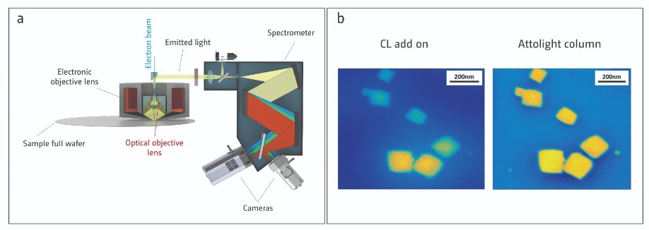
(a) The detection path in Attolight’s proprietary electron column features an aberration-corrected optical objective that is directly integrated into the electronic objective lens. (b) A key advantage of the aberration-corrected objective is that it ensures perfect homogeneity of the signal collected. This is illustrated in the image of the particles and the blue background, produced courtesy of P. Maurer and S. Chu, Stanford University.


