
Towards GaN-CMOS Technology without Regrowth
MIT team first to demo monolithic integration of p-channel and n-channel transistors based on GaN/AlGaN/GaN double heterostructure on 6 inch GaN on Si wafer
Researchers from Massachusetts Institute of Technology (MIT) claim to have broken new ground by being the first to demonstrate the monolithic integration of p-channel and n-channel transistors based on GaN/AlGaN/GaN double heterostructure on 6 inch GaN on Si wafer.
This demonstration paves the path towards the realisation of GaN-CMOS Technology without any regrowth. The researchers also demonstrated record low contact resistivity to p-type GaN which help them to achieve state of the performance for p-channel devices.
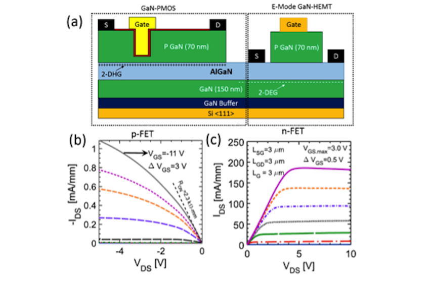
The picture above shows: (a) Cross section of the demonstrated monolithic n-channel and p-channel devices (b) Output characteristics of p-channel device (c) output characteristics of E-mode n-channel device.
To unleash the full potential of GaN technology for on-chip power switching applications, complementary transistors are needed to serve as high-speed gate drivers to the GaN power switches. Several groups around the world have demonstrated p-channel transistors that use polarisation-induced 2-dimensional hole gas (2-DHG) formed at the interface of III-N heterostructures.
However, a p-channel transistor that uses the epi-structure of p-GaN gated n-channel devices has not been demonstrated so far. In this recent work, such a p-channel transistor is fabricated and characterised on a commercially available 6 inch GaN on Si wafer. The demonstrated p-channel device used the same epitaxial structure like GaN based enhancement mode n-channel transistor (also known as Gate Injection Transistor), and therefore it does not require a regrowth process. In addition to that, the use of a Si substrate offers lower cost, availability of 200-mm-diameter substrates, and potential to integrate with dense logic and analog functionality.
The epitaxial stack is grown by Enkris Semiconductor on a 1-mm-thick Si (111) substrate using the MOCVD) method. The structure is as follows, 70 nm p-GaN (Mg: 3×1019 cm−3), 15 nm Al0.2Ga0.8N (Si: 5×1016 cm−3), 420 nm n-GaN (Si: 5×1016 cm−3), 4.2 μm buffer and Si substrate. The fabrication of p-channel device starts with the formation of the ohmic contacts to p-GaN for the source and the drain terminals following the a novel optimised process developed at MIT. Then the mesa etch is performed by Cl2/BCl3 based Inductively Coupled Plasma-Reactive Ion Etching (ICP-RIE) process using photo-resist mask.
A timed Cl2/BCl3 based ICP-RIE process is used to etch of p-GaN beneath the gate region using photoresist as the etch mask. Following the gate recess etch, the sample is dipped into heated TMAH in order to remove the photoresist and reduce the etch-induced roughness. After that Atomic Layer Deposition (ALD) is performed to deposit 17 nm of Al2O3 as the gate dielectric. Ti (20 nm)/Au (100 nm) gate metal is formed lift-off technique. For the n-channel device the team started by etching the p-GaN from the source and drain region. Then Ti/Al/NI/Au based ohmic contact is formed to 2-DEG by high temperature annealing. And then Ni/Au is deposited as the gate metal following the mesa etch.
DC measurement results of the fabricated p-channel devices show a ON/OFF ratio of ~105 with gate leakage in the range of 1 nA/mm. gm vs VGS characteristics demonstrates a peak transconductance of 135 μS/mm at VDS = −3.5 V and VGS = −3 V. Measured IDS vs VDS characteristics of the p-FET exhibit a RON of ~2.3 kΩ∙mm and on current of 1.1 mA/mm at VDS = −5 V and VGS = −11 V. The enhancement mode n-channel devices exhibit on current over 200 mA/mm and a threshold voltage of 1 V.
The major bottleneck of the proposed technology is the low-current density of the p-channel device. However, the current density of the p-channel device can be further improved by having a thicker AlGaN layer which would give rise to higher 2-DHG density. the researchers also have plans to grow a p++-InGaN layer on top so that they can achieve a very low ohmic contact to 2-DHG channel.
'p-Channel GaN Transistor based on p-GaN/AlGaN/GaN on Si' by N. Chowdhury et al; IEEE Electron Device Lett., vol. 40, no. 7, pp. 1036-1039, July 2019.


