

Colourful chip-scale microLED displays
Patterning epiwafers with indium-rich InGaN quantum wells enables the fabrication of monolithic, full-colour displays
BY HOI WAI CHOI, WAI YUEN FU AND HAO LYU FROM THE UNIVERSITY OF HONG KONG
The III-nitride family has provided us with many great devices. Thanks to this material system, we have: blue LEDs, which power solid-state lighting; violet lasers, which lie at the heart of Blu-ray optical data storage systems; and HEMTs, which are well-suited for high-power and high-frequency applications. What will come next? There is a good chance it will be the microLED display.
The reason why this is a strong possibility is that GaN LEDs are already used in large outdoor colour displays, assembled from red, green and blue LED modules with millimetre dimensions. The size of these modules makes it difficult to diminish the overall size of the panels, or reduce the pitch of the pixels. However, if this could be done, these devices could target the huge market for indoor displays. That includes televisions and monitors, which are predominantly based on LCD panels. To compete in this market, the size of each pixel must be 100 µm or less. This is the domain of the microLED.
TVs based on microLEDs have tremendous promise. Prototypes already exist, such as Sony’s 55-inch Crystal-LED, exhibited at CES2012, and Samsung’s The Wall, a highlight of the recent CES2019. Merits of this LED-based technology include a display that is self-emissive, so unlike that based on liquid crystals, it does not require a backlight. Such a display also allows for great blacks, the key to extremely high contrast, by selectively turning off microLED pixels. That’s a trait that is shared with OLED displays. However, microLEDs can switch faster, they cost less, consume less power, and are expected to be far more reliable in the long run.
The production of prototypes suggests that microLED displays are imminent. However, they might not be, given that there is yet to be a consensus on how they are to be built. Typically, red, green and blue microLEDs are fabricated at the wafer scale, before they are transferred to the display backplane with one of several techniques. Two of the most popular are ‘pick-and-place’ and ‘mass transfer’.
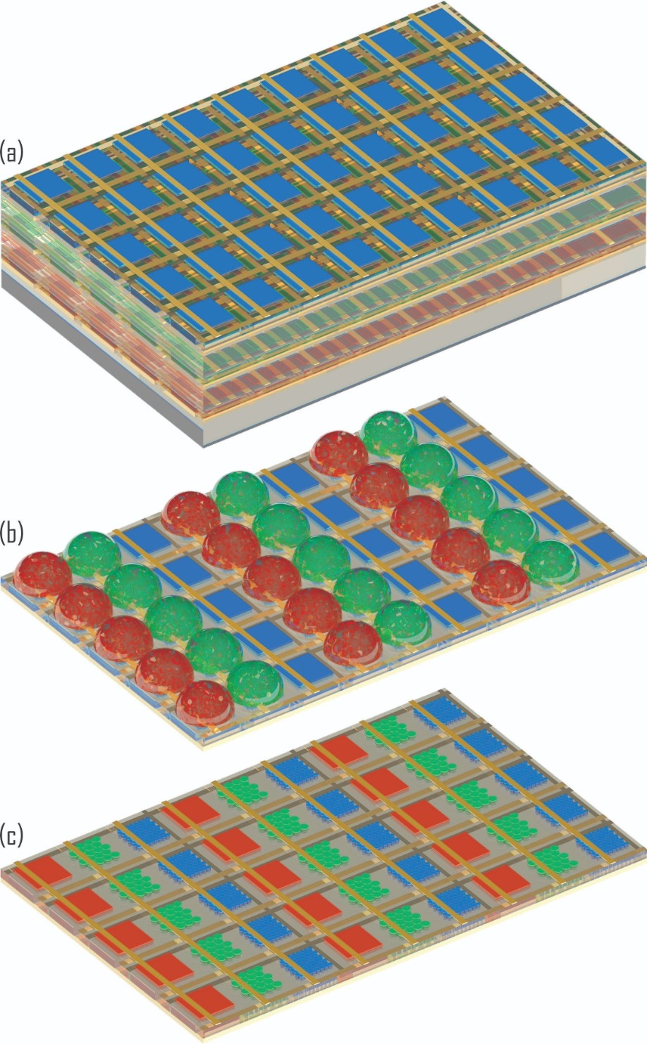
Figure 1. Schematics of proposed full-color microLED display by (a) stacking of red, green and blue microLED arrays, (b) selective phosphor coating, such as by jet-printing, on the red and green pixels of a monochromatic blue microLED array and, (c) monolithically integrating red, green and blue pixels on the same chip
Producing displays with this kind of approach is incredibly cumbersome, because so many red, green and blue LEDs have to be transferred to form a display. A full HD display requires 6 million LED chips, while four times this is needed to make a 4k display. These are massive numbers, on a par with the transistor count of the Pentium III microprocessor of the late 1990s. However, there is one crucial difference: those microprocessors were built using IC technology, with transistors monolithically integrated into a single chip using CMOS processes.Assembling millions of individual LEDs to make a microdisplay poses many challenges. Targets must be met for yield, throughput, placement accuracy, performance uniformity and manufacturing efficiency. These are requirements that are particularly challenging for high-resolution displays for handheld devices, because the dimensions of the microLEDs are just a few microns.
One of toughest requirements for making a microLED display is to eliminate dead pixels in a cost-effective manner. At first glance, a transfer yield of 99.99 percent is excellent, but this still equates to more than 2000 dead pixels on a 4k display. That’s simply unacceptable – the LCD displays of today have virtually zero dead pixels. Techniques for identifying and replacing dead pixels are being developed, but they contribute to manufacturing costs, reducing the chances of success in the hugely competitive display market. What’s more, mass-transfer processes impose a lower limit on the dimensions of the LED dies, and ultimately restrict the resolution of the microdisplay.
All these concerns highlight the need for a radically different production process, based on the use of IC technology for the manufacture of high-resolution GaN-based microLED displays. Adopting this approach would allow large numbers of devices and complex circuits to be batch fabricated on a single wafer, resulting in significant cost reductions as well as yield and reliability enhancements; the success of the silicon integrated circuits industry says it all.
If researchers pursue this approach today, they can draw on the development of microLED displays in the late 1990s. Back then, several research groups developed GaN microLEDs and microLED displays. These teams produced emissive microdisplays by forming monolithic arrays of micrometre-scaled LED elements, with pixels either addressed individually, or via a matrix. Being monolithic, such microdisplays are invariably monochromatic.
At the time, monochromatic microdisplays may well have been acceptable, as the mobile phones of that era often had mono-colour LCD displays. But now it’s an entirely different matter. In fact, consumers are not just looking for a colour display, but one of high-quality, with a wide colour gamut, a high contrast ratio, a quick response time and high brightness. Since many screens are mounted on mobile handheld devices, there is also a premium on a low power consumption.
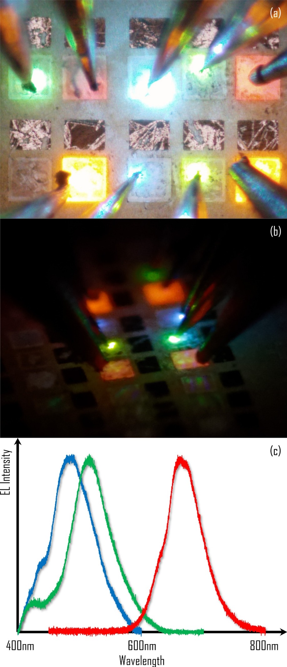
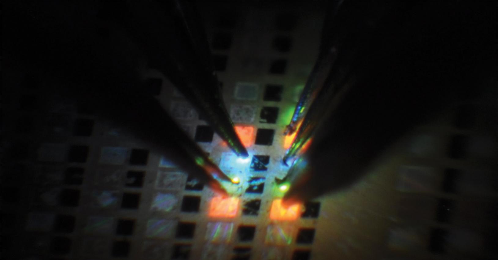
Figure 2. (a) Plan view and (b) isometric view photographs of a prototype for the monolithically integrated red, green and blue LEDs on the same GaN based LED wafer and (c) the corresponding electroluminescence spectra taken from the device.
Working towards this is our team from The University of Hong Kong. We have developed various technologies, based on heterogeneous integration, that could deliver full-colour displays. One of our ideas is to stack red, green and blue microdisplay chips on top of one another to form a full-colour microdisplay (see Figure 1(a)); and another of our conjectures is to selectively coat the pixels in our monochromatic monolithic microdisplay using, for example, jet-printing (see Figure 1(b)). However, both of these designs require complex fabrication processes. Consequently, they are only a little more feasible than a mass-transfer approach.To realise full-colour monolithic displays, the greatest challenge is the integration of multi-colour emitters from a single wafer. Sporadic reports have emerged of wafer-scale multi-colour emission, using various ‘bottom-up’ growth techniques. They include the growth of numerous sets of multi-quantum wells emitting at different colours within the same wafer, and the growth of nanostructures that feature either differing dimensions or different facets to generate various colours.
We tackle these fabrication issues from the opposite direction, pursuing a ‘top-down’ approach. Our starting point is the conventional planar GaN-on-sapphire LED wafer, which is compatible with conventional wafer process flows. On this we create nanostructures that induce spectral shifts. This enables us to generate colours that differ from that emitted by the multi-quantum wells. Ultimately, it allows us to make red, green and blue emitters that are monolithically-integrated onto the same chip or wafer.
The as-grown LED wafers that we start with produce single-colour emission, because the multi-quantum well structure is uniform across the wafer and the emission wavelengths from these wells are not tuneable. However, there is a possibility for bandgap tuning, arising from the highly-strained nature of the InGaN/GaN wells grown on c-plane sapphire. There is lattice and thermal mismatch during the growth of these layers, giving rise to the quantum-confined Stark effect, which is particularly prevalent in the indium-rich quantum wells that provide emission at longer wavelengths. Through dimensional downsizing of individual emitters, emission can be blue-shifted via strain-relaxation. This can deliver substantial changes – we have produced spectral blue-shifts of more than 100 nm, by forming nanostructured emitters with dimensions of less than 100 nm.
Our strategy is to form the micro-sized red, green and blue pixels by patterning an LED wafer featuring indium-rich, red-emitting InGaN quantum wells. The red-pixels are non-structured, so they emit at the as-grown wavelength of the wafer. Meanwhile, the green and blue pixels are formed by creating densely-packed arrays of etched nanostructures that provide strain-relaxation. For the blue-light emitting structures, the dimensions are roughly an order of magnitude smaller than those for their green-emitting siblings (see Figure 1(c)). To speed prototyping, we patterning our green and blue pixels using selective nanosphere lithography. This involves the deposition of silica nanospheres onto photolithographically-defined photoresist wells, either by spin-coating or ink-jet printing. Wafer-level processing is possible, by turning to nano-imprint lithography.
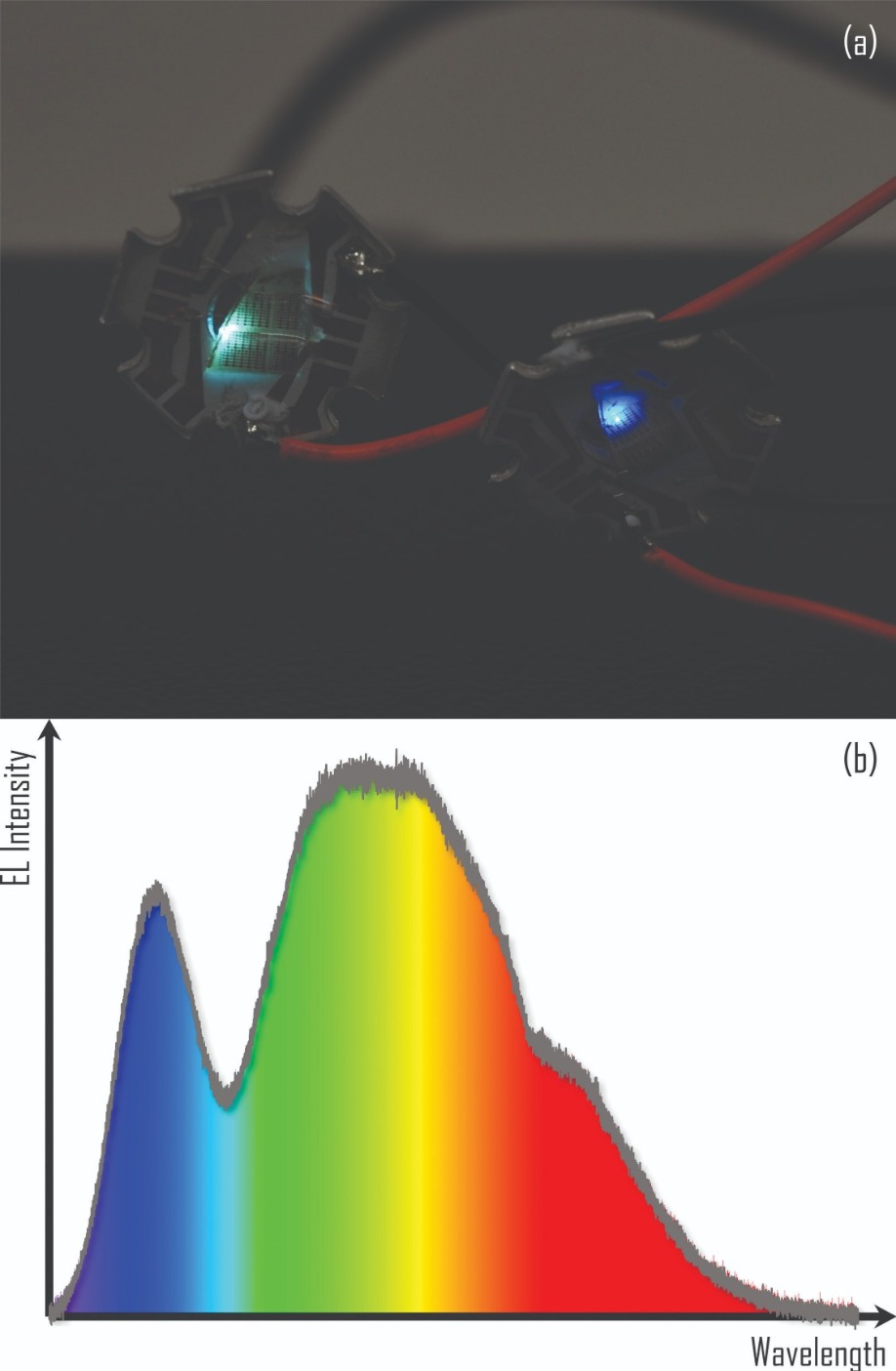
Figure 3. (a) Photograph of a phosphor-free white-light InGaN LED and (b) the corresponding electroluminescence spectrum
We form our nanostructures by dry etching through the silica nanospheres. This creates nano-pillars, which are subsequently passivated and planarized using spin-on-glass. The quantum wells within these pillars undergo strain-relaxation, leading to emission at far shorter wavelengths. By interconnecting the red, green and blue pixels in a matrix-addressable format, we are able to construct a full-colour microLED displays at the wafer-scale (Figure 2(a) and (b)). There are no limitations on scalability.
Plotting the emission spectrum from our wafers reveals three distinct peaks at 487 nm, 516 nm and 667 nm, produced by blue, green and red pixels, respectively (see Figure 2(c)). This successful demonstration of monolithically-integrated red, green and blue emitters underscores the feasibility of our approach for chip-scale fabrication of full-colour microLED displays.
We have also developed a phosphor-free white-light LED, using a similar approach. Rather than grouping red, green and blue emitters as individual pixels, we randomly distributed them across the emission region of the LED to create a white-light source (see Figure 3). By generating white light without the need for fluorescence, this source avoids the use of phosphor coatings, which drag down the efficiencies and lifetimes of today’s LED lightbulbs.
Of course, the proposed method is not without its drawbacks. Today’s indium-rich InGaN epiwafers have a low quantum efficiency, holding back the performance of the devices. However, we believe that efficiencies will improve in the coming years. This will support the successful commercialisation of full-colour microLED displays that are based on the monolithic approach that promises to increase yield significantly and shorten the processing time.
The monolithic integration technology that we have developed could also serve other applications. For instance, it could be used in a GaN photonic platform for on-chip communication, where fast microLEDs and photodetectors operating at multiple wavelengths could deliver a substantial hike in the data rates. This could be driven even higher with advanced multiplexing methods. Opportunities such as this make us very excited about the numerous functionalities and enhancements in performance that can follow from our development of microLEDs and their corresponding monolithic integration platform.
Further reading
H. W. Choi et al. IEEE Electron Device Letters 25 277 (2004)
“Semiconductor color-tunable broadband light sources and full-color microdisplays”, PCT Patent 2010/037274
“Method of making white light LEDs and continuously color tunable LEDs”, China Patent 101496188
C. Feng et al. ACS Photonics 3 1294 (2016)
“White nanoLED Without Requiring Color Conversion”, US Patent 9,401,453.


