

Making improvements with multiple materials

Better products result from etching GaN diodes from native substrates, uniting GaN HEMTs with passive devices formed on high-resistivity silicon, and growing III-Vs on silicon
BY RICHARD STEVENSON
No-one likes to compromise. It feels far better to select exactly what you want, rather than being constrained by your choices.
But in our industry, compromise is a common occurrence. You may crave the high power densities of GaN, but bemoan the low thermal conductivity of this wide bandgap material; or need the long-wavelength capability of the antimonides, but despair at the lack of maturity of this material system for high-volume production.
To improve this state of affairs, much effort has been directed at combining different semiconducting materials. This allows the merits of one to be allied with the strengths of another. Compromises still have to be made, but one gets far closer to the ideal.
Highlighting the gains that are possible with this approach are a handful of talks that were delivered at this year’s CS Mantech, held at Minneapolis, MN, from 29 April to 2 May. Speakers on this theme included Chris Youtsey from Micolink Devices, who revealed how cost-savings and superior thermal management result from removing GaN p-n diodes from their native substrate and transferring them to a copper carrier. In addition, Sangmin Lee from Wavice outlined how to use high-resistivity silicon as a foundation for integrated passive devices and GaN power amplifiers; and Amy Liu from IQE detailed how epitaxy can unite the low-cost, scalability and high level of integration of silicon with either the optical properties of InP and GaSb, or with the RF attributes of InP.
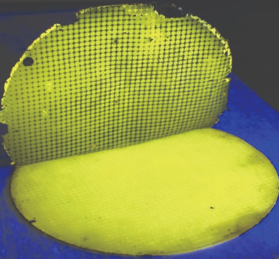
Figure 1. The team at Microlink have developed a photoelectrochemical etching technique that can remove a GaN epitaxial film from a 2-inch GaN bulk wafer.
Reducing thermal impedanceThe recent emergence of the large diameter, GaN substrate has spurred much effort in the development of vertical, GaN-on-GaN devices. Compared with those made from silicon, GaN-on-GaN diodes and transistors with this geometry promise multi-kV switching at far faster speeds and a substantially reduced on-resistance.
Off-setting these strengths, the GaN substrate has two major drawbacks. It is very expensive, hampering the commercial success of this technology; and it has a high thermal impedance, limiting the maximum power density and leading to larger die.
Addressing both these issues are Chris Youtsey and his co-workers from MicroLink Devices, working in partnership with engineers from Qorvo, Virginia Tech and the University of Notre Dame. By etching devices from the substrate and mounting them on copper, these researchers mitigate high production costs through substrate re-use; and they lower thermal impedance by attaching the chip to a copper carrier.
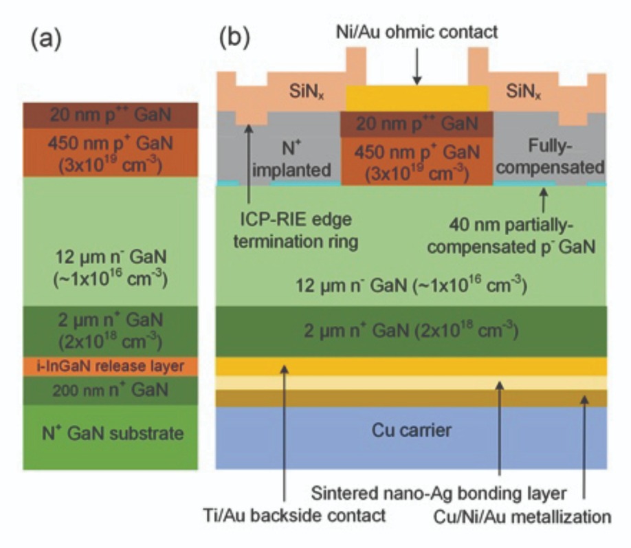
Figure 2. Microlink improves the thermal management of its GaN p-n diodes by bonding them to a copper carrier.
Youtsey believes that the re-use of the GaN substrate could enable substantial cost savings. “I think at least three to five reuses is possible. There is a cost associated with re-polishing GaN, but this will be a fraction of the cost of a new substrate.”He and his colleagues have spent many years developing and refining their photoelectrochemical technology for removing device structures from substrates (see Figure 1). However, it is only recently that they have applied this technique to the challenging task of separating a GaN device from its native foundation. “These [devices] require very high material quality and advanced device processing, incorporating effective edge termination, to achieve a low leakage current and a high breakdown voltage,” explains Youtsey.
Comparing the performance of the p-n diodes produced with this technique with those with a conventional architecture reveals that both designs have a nearly identical blocking voltage and ideality factor. However, the thermal impedance is cut by 30 percent with the transfer to the copper carrier.
“Note that the thermal benefits of epitaxial lift-off may be even more compelling than substrate re-use, since the layer transfer enables higher performance and reduced die sizes,” argues Youtsey.
The fabrication of the team’s diodes begins by loading HVPE-grown GaN substrates into an MOCVD chamber and depositing a sacrificial layer of un-doped InGaN, followed by a device heterostructure (see Figure 2). To support high-voltage operation, the engineers realise edge termination, using a shallow trench etch and a triple nitrogen implant. Evaporation and subsequent annealing at 600 °C adds low-resistance p-GaN ohmic contacts, and passivation results from the sputtering of silicon nitride. Evaporation of metal on the backside provides the n-type contact. For the control, the researchers use a Ti/Al/Ni/Au stack on the back of the wafer, while for the diode removed from the substrate, they use Ti/Au. Before starting the removal process, devices are encapsulated by sputter-depositing a TiW-Au seed and adding a 25 µm-thick support layer by electroplating. “Plating this thickness is not a major cost driver – maybe a few dollars per wafer,” says Youtsey.
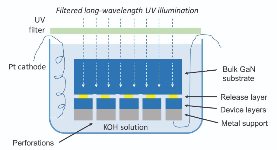
Figure 3. For the photoelectrochemical etching process, Microlink’s engineers use a platinum cathode. The sample acts as the anode.
Cross-shaped perforations are then defined in the metal support layer, and etched through the heterostructure to the release layer using wet and dry etching. To remove the sacrificial layer, the structure is placed in a beaker filled with a potassium hydroxide solution, with platinum and the sample used as the cathode and anode, respectively (see Figure 3). Etching frees the device when UV light is illuminated through the bulk substrate and absorbed in the InGaN release layer.After forming the released GaN foil, the n-type contact is blanket evaporated on the nitrogen face, before Kapton tape is applied to the top surface of the metal support layer (see Figure 4). The copper carrier is attached to the structure with a sintered nanosilver paste. After annealing at 260 °C for an hour, this forms a robust bond with high electrical and thermal conductivity. Finally, the Kapton tape is peeled off, before the metal encapsulation layer is removed by selective wet-chemical etching to the device structure.
Although quite a few steps are required to produce these devices, Youtsey believes that the additional processing is “not overly burdensome”, and he argues that it is justified by the benefits. He also points out that streamlining would take place before the technique entered production.
To support his claim for the suitability of the technique within a fab, he remarks that even with a conventional die-attach process, a full-thickness GaN substrate would have to be mounted on a temporary carrier, prior to backgrinding and the addition of a backmetal contact – and then there would be demounting, remounting to a tape frame, dicing, pick-and-place and die attach. With the technique he and his co-workers have pioneered, there is no need to backgrind, and dicing is simple, due to the thin foil that is held together by “tabs”. According to Youtsey, the additional process steps associated with the epitaxial lift-off process involve primarily etching away the metal encapsulation.
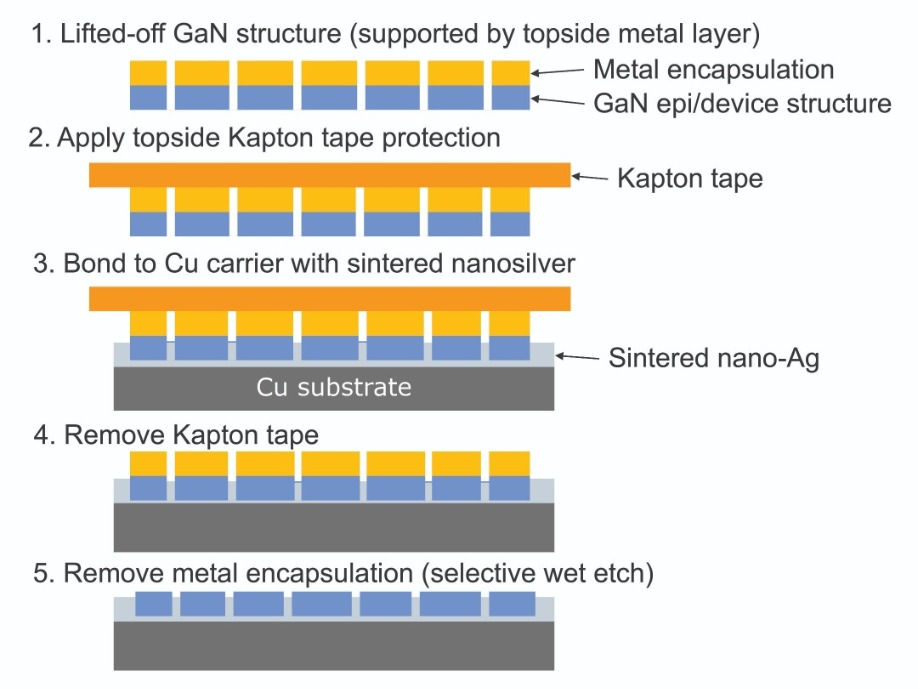
Figure 4. Micolink’s process flow for layer transfer and bonding of the released GaN foil.
Measurements of the diode on the copper carrier and the control show that both have an abrupt breakdown voltage at 1.3 kV, with failure stemming from imperfect edge termination, rather than defects within the diode region. The current-carrying capacity of the novel diodes exceeds that of the control. Those with diameters of 324 µm and 550 µm can pass 6.5 A and 10 A at a forward bias of 5 V. In comparison, at the same bias the control needs a diameter of 1 mm to pass 10 A, highlighting the potential for die reduction with the photochemical etching process.To assess the prospects for substrate recycling, the team reclaimed GaN substrates that had been used to make devices, and, in collaboration with Sumitomo Electric, removed about 50 µm of material with chemical mechanical polishing. Forming a p-n diode on this foundation and evaluating its performance with current-voltage plots shows that its behaviour is very similar to that of a device grown on a prime substrate.
Youtsey believes that the team’s technology has now reached critical mass, due to demonstrations of feasibility. “We are now engaged with several device manufacturers, and are actively looking for additional partners, with whom we can further develop and transfer the process into production.” According to him, the process has the potential to be used in the production of LEDs, microLEDs, VCSELs, photodiodes, laser diodes, and vertical power electronics.
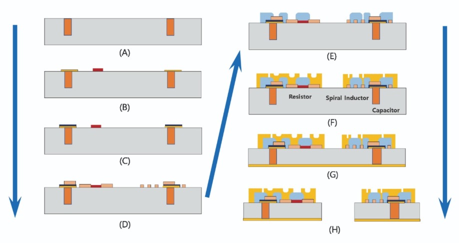
Figure 5. Wavice employs the following process flow for forming integrated passive devices on high-resistivity silicon with a via first, through-silicon-via process: (a) trench etch and copper fill, (b) NiCr resistor (red) and metal 1 (yellow), (c) SiN dielectric layer, (d) metal 2, (e) passivation, (f) metal 2 interconnect, (g) back grinding and metallisation, (h) singulation.
Compact, powerful amplificationThe roll-out of 5G infrastructure requires power amplifiers with a high output power, high linearity, high efficiency, low cost and small form factor. Although these performance criteria can be met with GaN MMICs, they are pricey, while the use of printed circuit boards fails to fulfil the need for a small footprint.
One promising alternative is the construction of quasi-MMICs, formed by hybrid integration of low-cost integrated passive devices and high-power amplifiers. Reports of this type of approach have emerged from universities, and now a manufacturing facility is following in these footsteps. Engineers at Wavice, Korea, have found by using this technology to surface mounting components on a board, they can slash the footprint for the unit from 30 mm by 30 mm to just 8 mm by 8 mm.
The starting point for this work is 525 µm-thick silicon substrates with a high-resistivity, because this trims the RF transmission loss. “It is standard, cheap, high-resistivity silicon,” says team spokesman Sangmin Lee. “We didn’t use high-purity, high-resistivity silicon.”
On this foundation Lee and co-workers create a 120 µm-deep trench, and fill it with electroplated copper, using TaN as a diffusion barrier. The purpose of this trench is to provide a through-surface via after the wafer has been thinned by back-grinding.
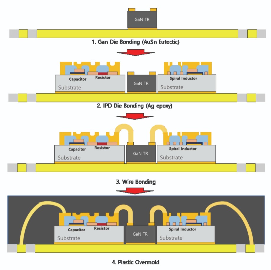
Figure 6. Wavice’s process flow for making quasi-MMICs by the hybrid integration of GaN HEMTs and integrated passive devices.
The next steps involve the addition of a silicon nitride film by plasma-enhanced CVD, followed by the creation of a NiCr resistor by sputtering and conventional lift-off. On this they add several metal and insulating layers, so that they can create capacitors between the first and second interconnect metals, and inductors between the second and third (see Figure 5).The backside of the wafer is then ground to a thickness of just 100 µm. This serves two purposes: it exposes the copper filled trench; and it ensures that the height of the integrated passive devices is the same as that of the HEMT. Integrated passive devices and HEMTs are then attached to the package base metal with a AuSn eutectic and silver, respectively (see Figure 6).
For the work reported in the CS Mantech paper, the team used a Wolfspeed CGH60008D for their GaN HEMT. Note, however, that Wavice also makes its own HEMTs. Its business model is to allow customers to choose between in-house HEMTs and those produced and by other suppliers.
Measurements on the package containing the Wolfspeed transistor reveal a peak power of 40.5 dBm. “It is about the maximum power from the device, which means no loss from the packaging,” says Lee.
During his conference talk, Lee showed the results of an X-band FET, featuring wafer-level packaging, high-resistivity silicon and a Wolfspeed CGHV1J0780D. That unit produced 52 dBm at 10 GHz. Lee says that higher powers are possible, but describes this level of performance as “reasonably good”.
The team are undertaking reliability testing of some of their quasi-MMICs. Assuming that the results are encouraging, the plan is for this technology – integrated passive devices on high-resistivity silicon – to be added to the company’s foundry service.
Additional goals include developing high-power amplifiers producing between 5 W and 30 W in the 2-6 GHz range, and a linear power amplifier with an average power of 5-10 W.
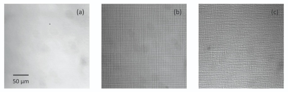
Figure 7. Normaski images of InP resonant-tunnelling diode structures grown at IQE. Images are for the devices structures grown on: (a) InP, (b) GaAs, and (c) and germanium-on-silicon.
III-Vs on siliconThe most attractive, but most challenging approach to uniting the III-Vs and silicon is epitaxial growth. Enjoying success is not easy, as there is a need to address lattice mismatch, while supressing the formation of anti-phase domain boundaries.
Doing just that is epiwafer supplier IQE, and at CS Mantech the company’s Amy Liu – who works at the Bethlehem, PA, site – offered an overview of the growth process the company has developed.
For this work, IQE uses (100)-oriented silicon substrates with a 6° off-cut toward [111], because this helps to supress the formation of anti-phase boundaries when the polar III-V material is deposited on non-polar silicon. Its other initiative to ease the transition from silicon to the III-Vs is to use a germanium transition layer, which has a similar lattice constant to that of GaAs.
The germanium layer is grown by CVD in an ASM E2000. Engineers then tend to switch to a Veeco GEN2000 multi- 6-inch production tool to add the GaAs layer, before transferring this epiwafer to either an Oxford-VG V-100 or V-150 production MBE system for the growth of the metamorphic buffer and the device layers predominantly based on InP.
Note, however, that it is possible to do this type of work by MOCVD. “We have demonstrated MOCVD growth process for InGaAs quantum well FETs on silicon, so we should be able to replicate other InP based devices also,” says Liu, who points out that the choice between MBE or MOCVD is governed by which growth process is best suited to creating the active device structures.
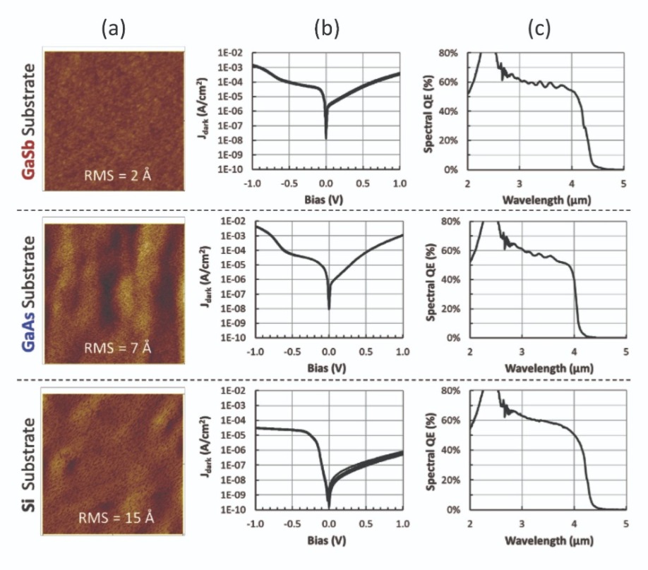
Figure 8. Engineers at IQE have grown the heterostructures for GaSb infrared photodiodes. Comparisons of atomic force microscopy images (a), current-voltage plots (b) and spectral response curves (c) are made for devices grown on GaSb, GaAs and silicon substrates.
One of the structures that Liu and her co-workers have grown on silicon is an InP-based resonant-tunnelling diode. This class of electronic device is faster than any other, making it a promising candidate for use in energy-efficient, compact, ultra-broadband, short-range wireless communication. In such systems, the resonant tunnelling diode could be used as a receiver.Supported by the EU project iBROW, the engineers at IQE have made resonant-tunnelling diode structures with an InGas/AlAs double barrier quantum well that feature an InAlAs metamorphic buffer, linearly graded to a high indium content.
The increase in lattice mismatch required to produce these InP-based structures led to strain relaxation. Epiwafers exhibit a slightly elevated surface roughness and a degree of cross hatching (see Figure 7). However, despite this degradation in morphology, this material is still able to produce resonant tunnelling diodes with their hallmark negative differential resistance.
Liu and her co-workers have also produced quantum cascade lasers. According to this team, this class of device delivers the highest performance in the entire medium-wave infrared and long-wave infrared spectral range. Constructing it on a silicon platform could open the door to low-cost, ultra-compact quantum cascade lasers for wireless communication, sensing and illumination.
At IQE, engineers have fabricated quantum cascade laser structures with 40 stages, each incorporating strained AlInAs barriers and InGaAs wells. The team had previously fabricated this structure on a GaAs substrate, with processed devices realising room-temperature lasing at 4.4 µm. Switching to a silicon substrate has proved challenging, partly due to the high degree of strain in the structure. The active region is designed to balance the internal forces, but the strain in the individual layers and any net residual strain adds to growth challenges.
Studying the surface morphology at various stages of growth revealed that this deteriorated with the addition of the active region. As one would expect, device performance and yield were impaired. However, these emitters were still able to deliver lasing at up to 170K.
After growing the resonant tunnelling diodes and quantum cascade layers, Liu and her colleagues started to see if they could improve the quality of the underlying germanium. They estimated that the threading dislocation density in the germanium is in the mid 107 cm-2, and they thought that the threading dislocation density in the InP layers would be about ten times this figure.
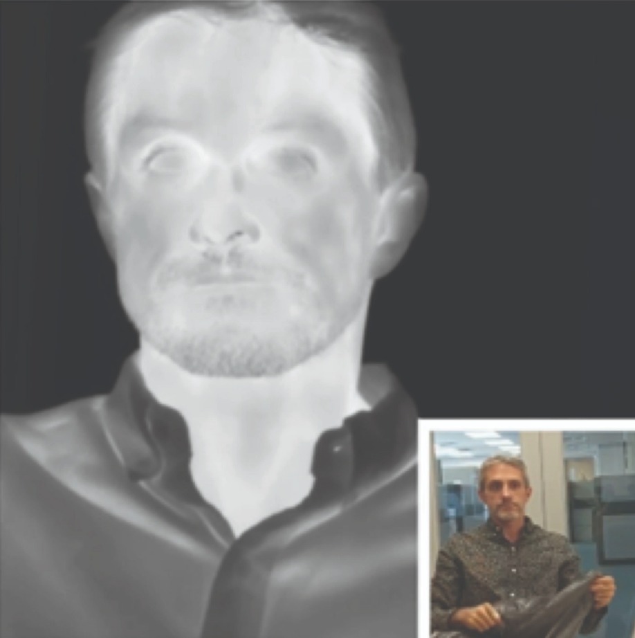
Figure 9. An infrared image taken from a focal plane array fabricated from an antimonide-based medium-wave infrared structure grown on a germanium-on-silicon template. The inset shows the corresponding visible image.
The traditional approach to determining the threading dislocation density is to inspect the material with cross-sectional and plan-view tunnelling electron microscopy. This is not ideal, however: it is time consuming, costly, the inspection area is limited, and it is unreliable when the threading dislocation density drops below 107 cm-2. To address all these issue, IQE’s silicon division has developed an in-house, wet-etching metrology technique. “It uses a proprietary etchant chemistry to effectively, easily, and quickly reveal etch pits on the germanium-silicon templates,” says Liu. According to her, the density determined by this technique correlate well with transitional threading dislocation density measurements, such as transmission electron microscopy.Using this in-house wet-etching metrology technique to assess threading dislocation density, Liu and co-workers undertook a programme to improve the quality of the germanium layer. Following several process modifications, this density fell to typically 5 x 105 cm-2.
The team have used the refined growth process to produce medium-wave infrared photodetectors, based on building GaSb structures on silicon substrates. This effort draws on previous work, involving the growth of metamorphic GaSb-based devices on GaAs substrates with a similar cut-off wavelength. When these structures were grown on 6-inch GaSb and GaAs substrates, they exhibited mirror-like surfaces, with roughnesses of 0.7 nm and 0.2 nm, respectively, according to atomic force microscopy. Switching to a silicon substrate led to a higher density of mounds, and an increase in surface roughness to 1.5 nm (see Figure 8).
However, even this increased roughness is acceptable for device fabrication. Detectors made from this heterostructure had a slightly higher dark current than equivalents incorporating the other two foundations, but they had a similar quantum efficiency – it’s 60 percent, even without an anti-reflection coating.
The structure on silicon has been fabricated into a focal plane array with 640 pixels by 512 pixels at QmagiQ of Nashua, NH, using a 15 µm-pitch process. Applying an anti-reflection-coating and moving to a fully packaged array propelled the quantum efficiency to 80 percent, with operability close to 100 percent. This is a level of performance able to provide high-quality imaging (see Figure 9).
One of the next goals for the team is to grow the InP-based resonant-tunnelling diodes and quantum cascade lasers on the improved germanium-on-silicon templates. This should lead to an increase in device performance.
“We also plan to continue our work on antimonide-based, infrared photodetectors on germanium-on-silicon templates, extending the work to longer wavelength devices,” explains Liu.
Such efforts will continue to showcase what is possible by uniting different material systems. It’s an approach that is not the norm today, but it’s becoming more common, and this trend seems set to continue.


