

In search of a new solvent
Although there is no universal successor to the widely used but increasingly outlawed solvent NMP, capable alternatives are coming to the fore
BY ANIL VIJAYENDRAN AND JOHN TADDEI FROM VEECO INSTRUMENTS
Some of the more common processes within the semiconductor manufacturing industry include positive photoresist stripping, developing and metal lift-off. For all these tasks, a very popular solvent is an organic compound with a five-member-ring that is known as NMP (or, to give it its full title, 1-methyl-2-pyrrolidone or 1-methyl-2-pyrrolidinone, N-methyl-2-pyrrolidone). NMP is effective in removing any photoresist residue while leaving the surface in good shape for downstream processing, and unlike some harsh solvents of the current era, it is not a carcinogen (although it is a reproductive hazard).
These advantages have helped NMP to become an industry standard, displacing a previous generation of solvents, thanks to superior chemical properties (see Table 1). Compared to a popular solvent of yesteryear, acetone, NMP has a far higher flashpoint – this allows processing below this temperature, improving safety.
In addition, NMP has a lower vapor pressure, leading to far lower emissions of volatile organic compounds, and recycling of this material can exceed 99 percent, even for pressurized dispenses. Yet another merit of NMP is that its photoresist saturation level is high, permitting processing of many wafers with recycled chemistry.
Within the compound semiconductor industry, NMP has made a name for itself as the preferred solvent for metal lift-off (see The merits of metal lift-off for details). However, it’s future could be short-lived. That’s because companies are looking to meet growing environmental health and safety requirements by decreasing the use of more harmful chemical formulations in compound semiconductor manufacturing.
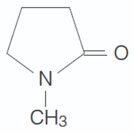
NMP, which has the chemical formula C5H9NO and a molar mass of 99.1 g/mol, has been used for wide range of applications, thanks to its great characteristics that include: a high flash point compared to similar solvents; the capability to mix with water in all proportions; miscibility with most organic solvents; a high boiling point, a low freezing point and being relatively easy to handle; and its chemical and thermal stability.
In fact, NMP has already been partially phased out in the EU, which has greater regulatory pressure than other regions around the world (see Table 1). Other countries are to be expected to follow this lead as worker exposure is a serious matter. Refinements to process tool design and selection can greatly reduce exposure for fab personnel, but avoiding the use of this particular solvent is clearly a more rigorous solution.In practice, up until now the concerns over environmental health and safety have generally been addressed with engineering controls in tool and fab design, and through real-time chemical monitoring of the air within the fab, to ensure that workers don’t get close to exposure limits. As well as a gradual shift away from manually operated equipment, there have been refinements to the airflow in wet process tools. Improvements include increased exhaust, multiple exhaust inlets, and the introduction of compartments within a tool, so particular chemistries can be segregated. In other words, worker exposure has been addressed by changing the tools performing the processes, rather than switching solvents.
Exploring alternatives
The use of NMP will not disappear overnight, as some established processes have been granted an exemption. However, many of the grandfather clauses are becoming increasingly difficult to extend, and there are already proposals in the US to restrict the use of NMP, following the lead taken by Europe.
Not everyone will lament the loss of NMP. This solvent – which is hygroscopic, so it picks up water from the air within the fab, affecting its pH – can corrode device metallisation. When deionised water is used directly to rinse the NMP from a patterned wafer, multi-metal stacks may suffer galvanic corrosion, detrimental to the wafer. One way to avert this is to carry out a preliminary rinse with isopropyl alcohol, but this increases emissions of volatile organic compounds and adds to solvent waste. So, in some fabs, alternative chemistries are used to process bump, pillar and redistribution layers.
One of the reasons why NMP will not be replaced overnight is that no-one has been able to identify an alternative chemical with all the desired attributes. The list of desired attributes for an alternative are extensive, as the replacement must be inexpensive, non-hazardous, non-volatile, fast acting, residue free, non-odorous, non-flammable, non-corrosive, and have a long life and a high saturation point for resist loading. Ideally, the new chemical that sports all these attributes would be supplied from an established chemical manufacturer, providing tremendous product support and a worldwide distribution network.
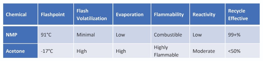
Table 1. Comparison of NMP versus acetone as a chemical used for photoresist stripping, developing and metal lift-off.
That’s a wish list that is not going to be fulfilled. There is no chemical with all the desired attributes, so there is no single replacement. Instead, process owners have to select a chemistry that fulfils the critical attributes required for their process, while complying with the constraints from their protocols.Coming to the aid of engineers within many compound semiconductor fabs is dimethyl sulfoxide (DMSO). It is compatible with existing wet process tool platforms; it can be used in a pure form; it is offered by a number of chemistry suppliers; and it can strip both positive and negative photoresist. In addition, it provides the main ingredient in many proprietary chemistry blends, and does not have not have the reproductive concerns of NMP.
Within the medical industry, DMSO is used to transport medicine through the skin and into the blood stream. That attribute is ideal for medical patches, but concerning for the semiconductor manufacturing industry. The danger is that when DMSO is used with harmful ingredients such as tetramethylammonium hydroxide (TMAH) – a commonly used base that is an autonomic nervous system toxin – it has the potential to transport this into a worker’s bloodstream via skin contact. Due to this, the environmental health and safety departments of some fabs are reluctant to permit DMSO as a substitute for NMP. This stance is not consistent, though. The medical use of DMSO highlights the benign nature of the chemical in its pure form.
The future of NMP
Removing NMP from legacy processes does not tend to involve the elimination of solvent processing; solvent processing is entrenched in the semiconductor industry, because it has proven to be a robust approach within the fabs. What’s needed is to identify another solvent that can replace NMP, and successfully perform the resist strip or metal lift-off process within the available toolsets.
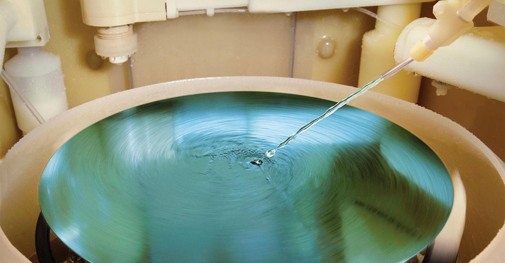
At Veeco, we have developed the PSP WaferStorm platform, a toolset that can ease this transition. Our equipment is designed not only for NMP, but can handle a wide variety of other solvents. Often the process times are similar to those that are used for NMP, so throughputs and process flows are hardly changed. But in some cases the processes are quicker, benefitting our customers.
To identify the methods to provide the best process results, our scientists and process engineers continue to work with many leading materials companies to evaluate the impact of different chemistries and equipment. We work with industry materials providers and process owners to qualify alternatives to NMP for chip production. The materials providers that we work with include EMD Performance Materials, Technic, Intelligent Fluids and Versum Materials. Thanks to these relationships, we are able to offer our customers a complete toolset, chemical and process solution.

Table 2. The timing to eliminate NMP varies by region.
The material suppliers that we work with are making much progress in providing alternatives to NMP. For example, EMD has developed the AZ KWIK Strip and AZ Removers 880, 910 and 920; Technic has successfully displaced NMP with its TechniStrip P1331 and TechniStrip Micro D2; and Versum Materials has developed Dynastrip AP7880-T.We will continue to evaluate candidates for replacing NMP at our demo lab in Horsham, Pennsylvania. Here, our efforts focus on developing processes and generating data. The insights that this provides help our customers to enjoy a smooth transition when implementing a new chemistry at their sites.
Within the compound semiconductor manufacturing industry, the most common method for patterning metal layers is to sputter or evaporate metal over patterned resist, and then undertake a metal lift-off step. The metal lift-off process begins by depositing a sacrificial material, such as a photoresist, on the substrate. The sacrificial material is then patterned, before depositing a metal on top of the substrate. After this, the sacrificial material is removed through exposure to solvent soaking and spraying. This leaves behind just the material deposited directly on the substrate.
Engineers may turn to metal lift-off processes when they need to pattern materials, but they cannot use etching, as this would damage the underlying materials on the substrate. Rather than using the acid-based etchants, which typically etch the compound semiconductor at a faster rate than the films on top of it, metal lift-off employs solvent chemistries which are compatible with these substrates. Another merit of metal lift-off is that the equipment required for this process is far less expensive than that for dry etching.
Today, depending on the process requirements, metal lift-off processes are carried out in wet benches or single-wafer systems. If the user has more challenging material to lift off, or strict chemistry usage requirements, single-wafer approaches tend to be preferred.


