

Gallium oxide: Laying the foundation for tomorrow’s success

Supporting the emergence of ultra-wide bandgap power electronics is the fast, high-quality growth of gallium oxide layers
BY Keith Evans, Gregg Dodson, Jacob Leach, Heather Splawn and Tamara Stephenson FROM Kyma Technologies
There is good reason to have concerns over the future of our planet. Average global temperatures are undoubtedly rising, due to increases in carbon dioxide emissions, and this trend could continue as energy demand climbs.
Against this bleak backdrop, two rays of hope are the increases in energy generated by renewables, such as wind and solar, and the tremendous potential for the electric car. In both these cases, improvements are possible by increasing the efficiency of power electronics. Succeed on this front and more energy will be fed into the grid from renewables, by increasing the efficiency for stepping up and down voltages and converting them between their AC and DC forms; and there will be an increase in the efficiency with which the energy from the car battery is converted into a form that drives the wheels. The latter is a major plus point – it trims the automobile’s running costs and boosts its driving range, gains that could lead to increased sales and ultimately better economies of scale.
Today, the majority of incumbent power devices are made from silicon. This enables low-cost manufacturing of diodes and transistors. However, silicon’s intrinsic properties are overshadowed by those with a wider bandgap, notably SiC and GaN. These rivals have greater critical fields, primarily due to their larger bandgaps, and this allows them to excel in all the key figures-of-merit (FOM): Baliga’s FOM, Baliga’s high-frequency FOM, Johnson’s FOM, and Keye’s FOM. These higher FOM enable SiC and GaN devices to block higher voltages, more efficiently switch electrical current on and off, and more efficiently pass electrical current when the switch is in the on-state. Due to all these virtues, wide-bandgap materials offer energy-efficiency savings over silicon in all power electronics applications.
Recently, these devices have come a long way. Rewind the clock to the end of the previous decade, and nearly all of the SiC and GaN power electronics development was taking place in R&D labs. But in the intervening years this has changed dramatically, with devices reaching a state of maturity that has led to commercial traction, particularly for SiC.
Sales are accelerating due to the great gains in performance, such as a 90 percent reduction in efficiency losses during electric-power switching, which can take place during regenerative braking in hybrid and all-electric vehicles and in electric converters connecting wind farms to the grid. But that’s not the only significant attribute of these wide bandgap power devices. Unlike those made from silicon, they don’t need cooling to work well. In addition, they can be made smaller, to feature in circuits operating at higher switching frequencies that contain smaller passive components. The upshot is smaller, more efficient units that require less cooling and are more reliable and robust.
From wide to ultra-wide
These wide bandgap materials are taking the power electronics industry on a journey that may not stop with SiC and GaN, but continue onwards, to a class of materials known as ultra-wide bandgap semiconductors. These lesser-known materials, which include AlN, AlGaN, Ga2O3, and diamond, promise to deliver further advances in the size, weight and efficiency of electrical units (see Figure 1 for a plot of unipolar electronic device figures-of-merit for silicon, GaAs, 4H-SiC, GaN, b-Ga2O3, AlN and diamond).
At Kyma Technologies of Raleigh, NC, we are developing an ever-expanding portfolio of technologies related to wide bandgap and ultra-wide bandgap materials. Our efforts include the development of crystal growth processes and tools for making these materials. We are routinely growing AlN, AlGaN, GaN, Ga2O3, and diamond materials; and we are routinely fabricating GaN devices.
Our current programme includes the development of Ga2O3 devices. We have mastered the growth of high-quality, n-doped films of Ga2O3 by HVPE, and our next challenge lies with device development.
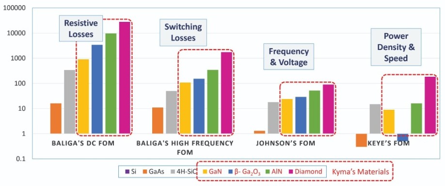
Figure 1. Four common unipolar electronic device figures-of-merit (FOM) for silicon, GaAs, 4H-SiC, GaN, β-Ga2O3, AlN, and diamond. Kyma’s materials in development or for sale are identified by the red dashed lines.
If ultra-wide bandgap materials are to fulfil their potential, manufacture must involve large-area substrates, used to produce high-quality epiwafers at high growth rates. Large-area substrates are a pre-requisite to success, as they drive up manufacturing efficiencies and slash the cost of every device produced. It is for this reason that silicon technology has progressed from research on 1-inch wafers to production on initially 100 mm wafers, and then on to those with diameters of 150 mm, 200 mm and 300 mm. That’s not the limit – 450 mm wafers exist today, but are yet to be used widely. When it comes to epitaxy, a key requirement for manufacturing vertical devices is the growth of thick, controllably doped n-type drift regions on large-area substrates. This has to be accomplished at the lowest possible cost of epitaxy per unit area. Due to all the reasons outlined above, when we develop our technologies, we make sure that they are compatible with large-area materials and ensure high-purity, high-rate growth.Our Ga2O3 products include β-Ga2O3 substrates, homoepitaxial β-Ga2O3 epiwafers, α-Ga2O3 epiwafers grown on sapphire substrates, and crystal growth tools for growing those epiwafers (see Figure 2 for an overview). Thanks to our vertically integrated approach, we can control the final finish of the substrate before engaging in epitaxial overgrowth. We offer this as a service too. Customers can supply us with their substrates, and even their grown epiwafers, and we can polish them. In addition, if desired, we can impart a defined mis-cut.
For more than 15 years, we have been using HVPE to grow GaN, AlN, and AlGaN materials. Back in late 2015 we decided to convert one of our GaN HVPE tools so that it could be used to grow homoepitaxial β-Ga2O3 epiwafers for a partner of ours that supplied the substrates.
Making the transition from growing GaN to Ga2O3 went against the grain. For many, many years, oxygen has been our enemy, but now it was needed to be more prevalent in the crystal than gallium, if we were to be successful. This transition posed many questions. Did we need to add a purified oxygen source to our tool, or would clean dry air suffice? How vulnerable would our GaN-optimised tool be to the generation of particulates in the form GaxO1-x? And would the high degree of chemical purity that is realised with our GaN growth process also lead us a high chemical purity in Ga2O3 growth capability?
Fortunately, we had help in answering all these questions. There is a wealth of information in the literature – we thank especially the incredible researchers in Japan for sharing their findings, by publishing their exciting results in all aspects of Ga2O3, including the application of HVPE technology. These insights have helped us to establish a HVPE process for producing high-quality homoepitaxial β-Ga2O3 and heteroepitaxial α-Ga2O3 films at growth rates ranging from 2 µm/hr to 20 µm/hr.
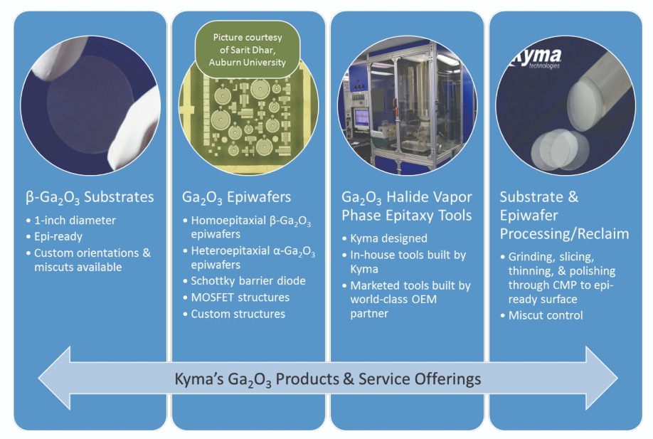
Figure 2. Kyma’s Ga2O3 related products and services.
We have found that when growing β-Ga2O3 films by HVPE, getting the right substrate preparation and offcut angle is critical to getting a good surface morphology and a high-quality epilayer. It is difficult to detect sub-surface damage on a freshly prepared β-Ga2O3 substrate, but any imperfections that are there give rise to morphology issues during HVPE overgrowth of β-Ga2O3.Compromised material quality is evident in the linewidths of X-ray diffraction scans (see the table in Figure 3). These results have helped us to improve our polishing process, so that it is capable of adequately removing sub-surface damage. The result is a relatively flat surface, according to atomic force microscopy (see Figure 3(a)), and a far better surface after HVPE growth of β-Ga2O3 films (compare the optical microscopy images in Figure 3 (b) and (c)).
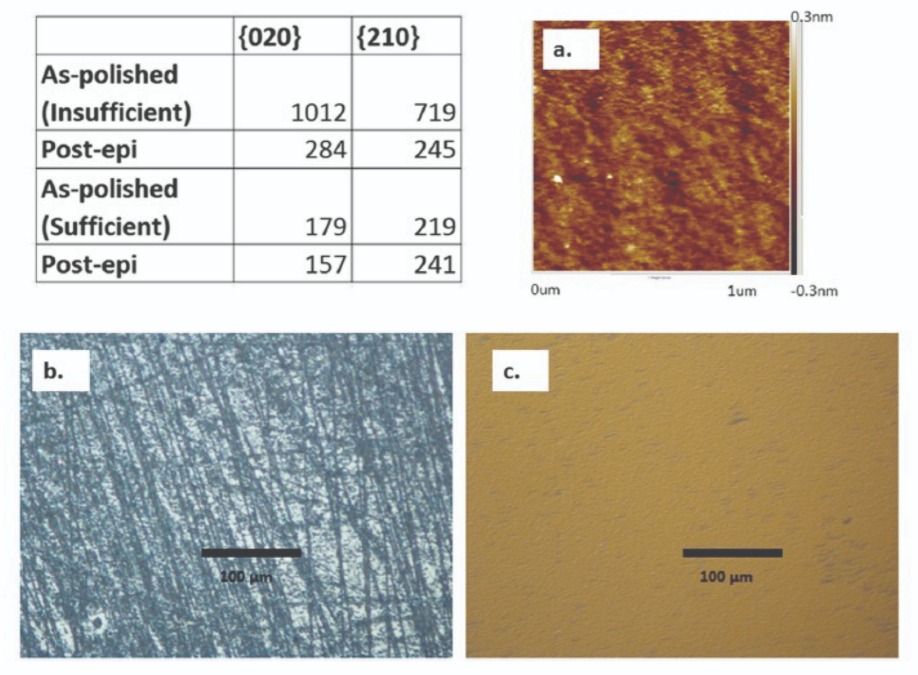
Figure 3. Table of X-ray diffraction arcsecond linewidths, defined as the full-width at half-maximum, for as-polished wafers and post-HVPE films using insufficiently polished and sufficiently polished processes. (a) 1 x 1 µm AFM image of a polished (010) β-Ga2O3 substrate and optical microscope images after 0.5 µm of homoepitaxial β-Ga2O3 growth using (b) an insufficiently polished and (c) a sufficiently polished substrate.
Optical microscopy also highlights the influence of the surface off-cut on the epilayer surface morphology. We have used this technique to compare the surface morphology of two homoepitaxial β-Ga2O3 films grown under identical growth conditions at 1000 °C. The pair of substrates we have used are nominally identical bulk (010), but one is on-axis and the other mis-cut by about 2° in a preferred direction. Images, collected by a rapid-inspection tool provided from Nanotronics that is equipped with nSPEC artificial intelligence, clearly show that a mis-cut substrate results in superior surface morphology (see Figure 4).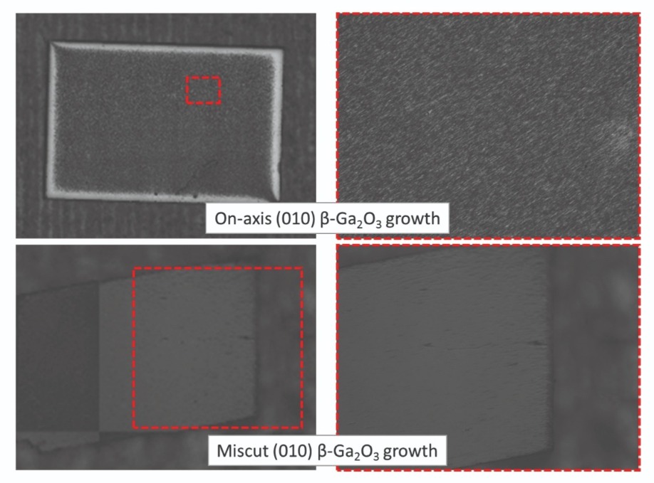
Figure 4. Optical microscopy images of β-Ga2O3 films obtained using the nSPEC artificial-intelligence-enabled, rapid-inspection tool that Kyma brought in-house in 2013. This tool serves as a workhorse, used by Kyma to measure almost every epiwafer or substrate made, and to scrutinise many incoming materials prior to use. Lower magnification images on the left and higher magnification images on the right show a much smoother film morphology for homoepitaxial β-Ga2O3 growth on properly mis-cut substrates (bottom), when compared with growth on on-axis substrates (top).
Having addressed optimisation of the surface mis-cut, eliminated sub-surface damage, and optimised the growth chemistry, we have gone on to produce a range of n-type homoepitaxial β-Ga2O3 films with differing electron concentrations. Assessing them with Hall effect measurements reveals that as electron concentration falls from around 1019 cm-3 to 1017 cm-3, mobility decreases from around 90 to 120 cm2 V-1 s-1 to around 50 to 60 cm2 V-1 s-1. Grow rates are controllable, for the range 2 to 20 µm/hr.
Figure 5. Room temperature mobilities vary with electron concentration in films grown on bulk β-Ga2O3. Triangles and diamonds represent films grown under identical conditions, except that the diamonds represent intentionally silicon-doped films, while the triangles represent unintentionally doped films. The open triangle and open diamond represent growths on bulk substrates with higher structural quality – these epilayers exhibit linewidths of less than 100 arc sec for {020} reflections.
We have also investigated the growth of films of α-Ga2O3. Compared to its thermodynamically stable sibling α-Ga2O3, this polytype is metastable, has a higher crystalline symmetry and sports a wider bandgap, making it an interesting choice for device applications. It major weakness is that it cannot be grown from the melt, so films of α-Ga2O3 have to be grown on a non-native substrate.Sapphire is the obvious choice, given that α-Al2O3 is the thermodynamically favoured form of crystalline Al2O3, and that it is possible to grow α-Ga2O3 on α-Al2O3. As is the case with homoepitaxial β-Ga2O3 films, surface preparation is essential for growing high-quality films. Evidence from optical microscopy highlights this requirement, clearly exposing the difference in morphology between α-Ga2O3 grown on c-plane sapphire substrates that have been properly and improperly polished (see Figure 6). Optimise the substrate’s surface, and it’s possible to realise excellent surface morphology.
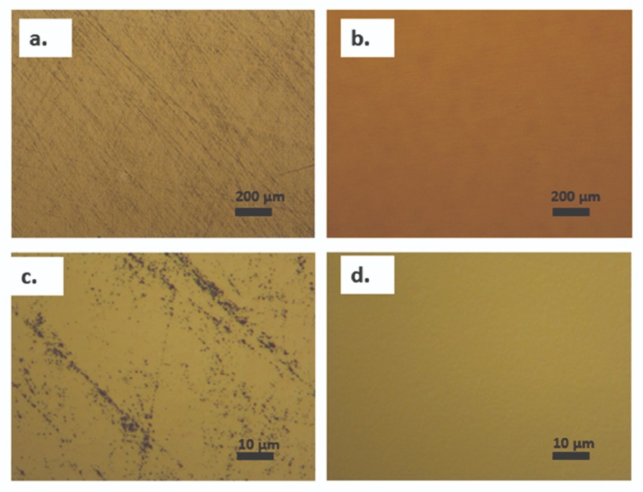
Figure 6. Microscope images of 1 µm-thick films of α-Ga2O3 at: 20x, for (a) and (b); and 100x, for (c) and (d). The film grown on the properly polished substrate, imaged in (b) and (d), has a far better surface morphology than that shown in (a) and (c), images of the film grown on the unsuitably polished substrate.
We have made significant strides with Ga2O3. We’re pretty excited that we now have good control over substrate preparation, growth chemistry, n-type doping, surface morphology, and background doping. These capabilities are going to lay the foundations for our move to device development. We believe that of the two polytypes of gallium oxide, it is β-Ga2O3 that has the greatest potential to gain commercial acceptance, especially in high-voltage power switching. Yet because β-Ga2O3 on α-Al2O3 has the advantage of a more mature substrate supply chain, we’ll remain active in that approach as long as our customers support it. We hope to play a role in bringing each of these technologies to market over the next few years.J.H. Leach et al. APL Mater. 7 022504 (2019)


