

Supercharging the HEMT

Cranking up the aluminium content in the AlGaN channel promises to create high-power HEMTs for extreme operating conditions.
BY Patrick Carey, Fan Ren AND Stephen Pearton FROM THE UNIVERSITY OF FLORIDA AND Albert Baca, Brianna Klein, Andrew Armstrong Andrew Allerman and Robert Kaplar FROM Sandia national laboratories
Power electronics are ubiquitous. They are deployed in satellites, unmanned autonomous vehicles, electric cars, photovoltaic systems, and power transmission on the utility grid.
Silicon is still the dominant material for making these power devices, but in the last decade or so there has been an increasing use of wider bandgap materials, such as SiC and GaN. This move has much merit: it opens the door to higher switching frequencies and superior thermal management; and it slashes the size and weight of the power converter, by allowing the use of smaller, lighter passive elements while simplifying thermal management.
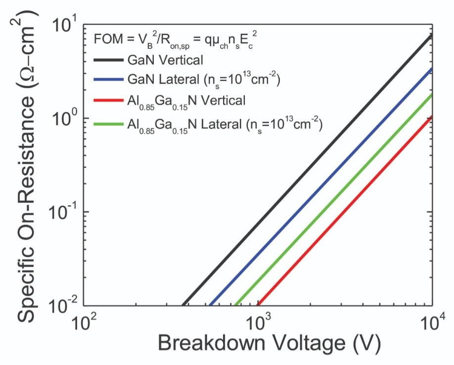
Figure 1. Specific on-resistance versus breakdown voltage for high-aluminium-content devices compared with GaN.
The introduction of SiC and GaN devices is not going to be the end of the story, but the beginning of a journey to materials with even wider bandgaps. Under development right now are devices made from ultra-wide bandgap semiconductors, such as diamond, Ga2O3 , BN and high-aluminium-content AlGaN. This class of materials promises to propel device performance to a new level.In applications where devices are deployed in an extreme environment, high powers have to go hand-in-hand with greater robustness. These attributes may be required in avionics, automotive, nuclear, defence, and extra-terrestrial applications. For example, in exploratory missions to the surface of Venus, devices must withstand temperatures of 500°C, while maintaining their performance in corrosive sulfuric acid clouds. In addition, there can be the need to provide continuous operation when bombarded by radiation. The Galileo orbiter, which probed Jupiter
for many years, withstood an irradiation dose above 600 krad before it plunged to its planned demise as the effects of radiation damage became unrecoverable.
Traditionally, it has been the wide bandgap materials SiC and GaN, working in conjunction with other technologies, that have provided a reasonably successful approach to extending device lifetimes in these high-power applications operating in extreme environments. But these materials are beginning to reach maturity, so obvious questions arise. Two that top the list are: What is the next material system for power electronics? And what will be the next innovation?
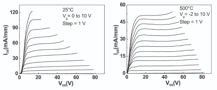
Figure 2. Typical current-voltage characteristics at 25 °C and 500 °C.
Every ultra-wide bandgap semiconductor has its pros and cons. Often there are concerns related to cost, substrate availability, and existence of controlled doping and contact schemes. For example, while Ga2O3 has made some progress in vertical diodes with bulk growth technology, its low thermal conductivity, lack of native p-type doping, and low electron mobility are drawbacks for its use in power electronics.An attractive option is to build on the success of previous efforts. That’s possible with GaN, a material that has benefitted from more than thirty years of exploration and investment. Its performance can be improved by increasing the aluminium content in the AlGaN channel of the HEMT. That’s the approach trailblazed by our team, a partnership between the University of Florida and Sandia National Laboratories.
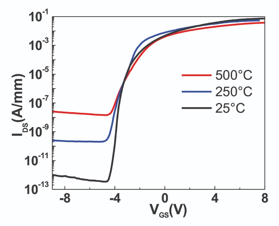
Figure 3. Id-Vgs curves at select temperatures from 25 °C to 500 °C.
One of the greatest strengths of AlGaN is its ultra-wide bandgap, which leads to a very high critical breakdown field, Ec. The exact relationship between the critical field and the bandgap, Eg, is a focus of active research, but it is essentially a power law,with Ec proportional to Eg2.5. Due to this relationship, when the aluminium content increases to 70 percent or more, the bandgap widens to 5.4 eV, and the breakdown voltage increases – it should hit 13.4 MV/cm (see Figure 1 for a comparison of aluminium-rich devices and those with pure GaN, illustrating the potential for devices that combine an ultra-low specific on-resistance with a high breakdown).
Like other ultra-wide-bandgap materials, alloys of aluminium-rich AlGaN hamper the production of low-resistance ohmic contacts. In addition, with this ternary it is challenging to realise meaningful carrier concentrations and high mobilities. However, excellent progress has been made to date in all these areas.
Encouragingly, initial irradiation studies on HEMTs with high-aluminium-content AlGaN-channels show that bombardment with 2.5 MeV protons has little effect on this device. However, research prototypes show a reduced single-event burnout tolerance in simulated space environments.
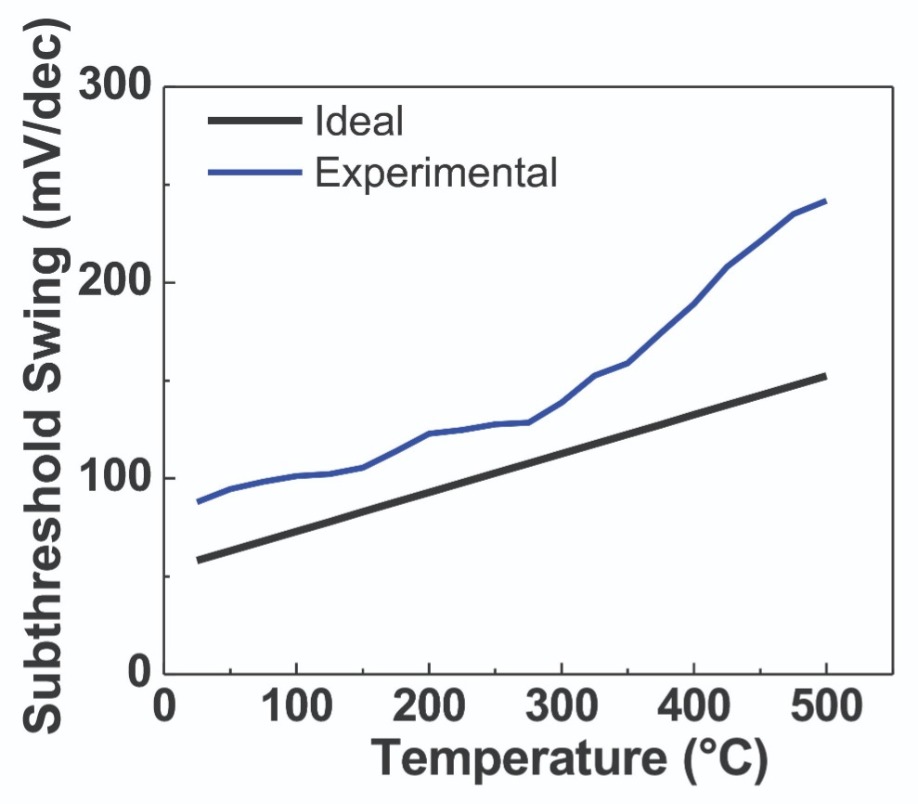
Figure 4. Experimental and ideal subthreshold swing as a function of temperature.
These results indicate that there is an improvement in total dose irradiation hardness when moving from a GaN-channel device to an AlGaN HEMT. This is to be expected, given the strength of the atomic bonds. For GaN, it is 8.92 eV/atom, while for AlN, it is 11.52 eV/atom – to put those figures in context, values for silicon and GaAs are just 2.34 eV/atom and 2.17 eV/atom, respectively.Growing AlN
For every compound semiconductor, it is ideal to grow the epilayer on a native substrate. So, for AlN HEMTs, the perfect platform is high-quality, single-crystal AlN. This foundation has a bandgap of 6.2 eV, a high thermal conductivity of 285 W m-1 K-1, and it provides a nearly lattice-matched substrate for aluminium-rich AlGaN epilayers, greatly reducing strain and threading dislocation density in this ternary.
Producing high-quality AlN substrates is very challenging. The most promising method for preparation, physical vapor transport, produces material with dislocation densities below 103 cm-2. However, commercialising substrates with this technique is far from easy, as it is tricky to combine a sufficient size with a low defect density.
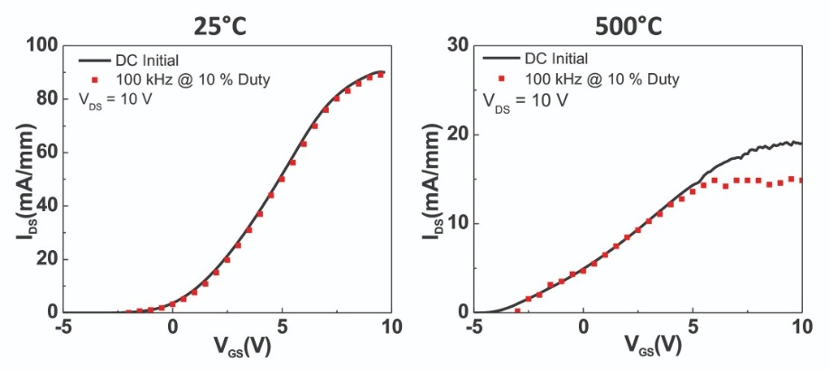
Figure 5. Gate lag at 25 °C and 500 °C performed at 100 kHz, 10 percent duty, and a drain-source voltage of 10 V.
Due to the high cost of AlN substrates, the majority of efforts directed at developing AlGaN are undertaken with sapphire or SiC substrates. They provide a template for growing a layer of AlN, which provides the foundation for AlGaN devices.Growing AlN on sapphire is not straightforward. Two of the greatest issues are the large lattice and thermal conductivity mismatches. Failure to take sufficient care leads to cracks developing in AlN grown on sapphire after the critical thickness has been reached, due to tensile stress from the coalescence process.
Much effort has been devoted to avoiding this, and after 15 years of detailed study of the epi-growth of AlN epilayers on sapphire, there are now several reports that detail different growth processes for producing device-quality AlN epilayers.
When AlGaN epilayers are grown on AlN-on-sapphire templates, it is the composition of the AlGaN that determines epilayer, lattice and thermal mismatch. These mismatches can be exacerbated between the AlGaN and AlN. To reduce the stress and the density of defects in AlGaN epilayers, engineers can turn to compositionally-graded layers or superlattices, or begin by intentionally inducing three-dimensional growth modes, before switching to two-dimensional growth for planarization.
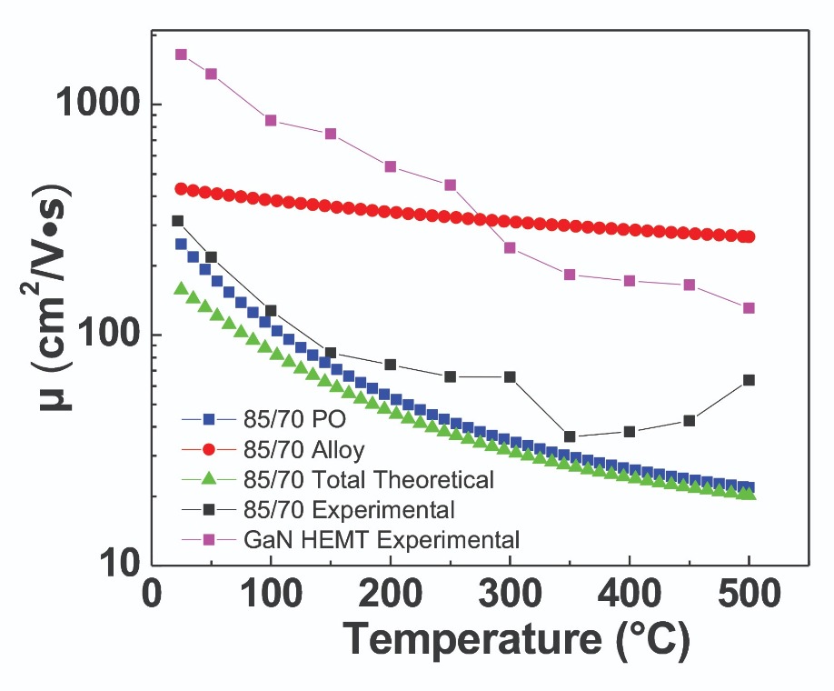
Figure 6. Modeled and experimental electron mobility as a function of temperature for the 85/70 HEMT, compared with a traditional GaN HEMT.
Processing challengesOur team has used MOCVD to produce aluminium-rich AlGaN HEMTs on sapphire. The typical composition for these structures is a 85 percent aluminium barrier layer and a 70 percent aluminium channel layer. We refer to this structure as 85/70.
With these compositions, the epilayers can behave as insulator-like materials, hampering the formation of ohmic contacts. Regardless of metallisation and annealing temperature, it is difficult to achieve linear, low-resistivity contacts without employing more advanced techniques. Our simple planar contacts have realised a contact resistivity of 2 × 10⁻² Ω-cm2. While this resistivity is still far higher than 10-6 or less, a typical range of values that are easily achieved in GaN devices, we believe that it is quite reasonable for an early attempt with our new aluminium-rich materials.
One established process for the AlGaN HEMT is plasma etching, a technique that is widely used with GaN. It is relatively easy to etch tens of nanometres per minute, a rate that optimises the control of the recessed gates. There is a danger that surface roughness can arise from micro-masking of the surface of Al2O3. However, this can be prevented with an appropriate gas chemistry to produce surfaces with a root-mean-square roughness below a nanometre. We have found that a small addition of BCl3 assists in the removal of Al2O3, to yield a better surface than that realised with a pure Cl2/Ar environment.
Trumping GaN
We have evaluated the performance of our 85/70 transistor from room temperature up to 500°C. Measurements of the forward current as a function of voltage reveal full gate modulation across the entire temperature range (see Figure 2). A great attribute of these devices is that they produce full pinch-off up to these temperatures. In sharp contrast, GaN HEMTs fail to provide full pinch-off above 300 °C – and they are plagued by a poor current on/off ratio, which is typically around 104.
One characteristic of SiC and GaN devices is a current-voltage curve with an upward slope in the saturation regime at elevated temperatures. This behaviour is not ideal – the slope should be horizontal – and it indicates a low output resistance, which hinders high-temperature performance. The is not an affliction for our 85/70 devices, which have a reasonably horizontal current-voltage slope in the saturation regime at 500 °C. This unique performance provides a significant improvement over traditional GaN-channel HEMTs.
At very high temperatures, the quality of the gate dictates channel modulation characteristics. We have undertaken initial studies with a Ni/Au gate. At room temperature, the Schottky barrier height is a moderate 1.2 eV, a value comparable to that of a GaN HEMT at room temperature. Raise the temperature, however, and device performances diverge. For our 85/70 device, the barrier height of the gate appears to be entirely unpinned, with a magnitude increasing to 3.3 eV at 500 °C. The lack of pinning is highly desirable, as it implies that the electrons on the gate gain thermal energy under heating, while in tandem the barrier height increases in magnitude, preventing an excessive leakage current at high temperatures. Another advantage of the high Schottky barrier is that it allows AlGaN devices to be driven at higher current densities and at higher drain voltages than GaN equivalents. The level of superiority is particularly acute at elevated temperatures.
It is worth noting that the unpinned behaviour may not hold true for other gate metal stacks. We are investigating this as we explore different designs to further improve device performance.
A significant benefit that stems from turning to high-aluminium-content AlGaN is the increase in breakdown performance. Efforts by our team reveal that AlGaN HEMTs are capable of withstanding electric fields up to 2.5 MV/cm, a figure that is approaching the SiC limit. Far higher values may be possible, as we are yet to employ techniques to improve performance, such as a source field plate, and it is still early in the development of this material system. For example, we have not yet begun to explore better dielectrics to match the breakdown field of AlGaN. Our hope is that as the growth, the device design, and the processing are optimised over the coming years, fabricated devices will move closer to the theoretical limit of 13.4 MV/cm.
Better breakdown characteristics are very valuable, as they drive down the power loss of the device that is associated with the reverse leakage current. For our devices, the current is as low as 10-12 A/mm at room temperature, rising to just 10-8 A/mm at 500°C (see Figure 3).
These plots of reverse leakage at different temperatures can be used to determine an activation energy, and ultimately the mechanism behind the drain leakage current. Using an Arrhenius plot, we have determined an activation energy of 0.63 eV for temperatures below 350 °C, and an activation energy of 0.076 eV above 350 °C. An activation energy of 0.63 eV is consistent with Poole-Frenkel emission, while that at 0.076 eV is associated with band-to-band tunnelling. This can take place at this low energy due to significant bending within the conduction and valence bands.
The other key metric that can be extracted from these current-voltage plots is the sub-threshold swing. At room temperature, our devices have a value of 80 mV/dec, not far from the ideal 60 mV/dec (see Figure 4).
From these graphs of sub-threshold swing we are able to extract the interfacial trap density. It is clear that there are two distinct linear regions: one from 25 °C to 300 °C, associated with trap densities of 2 × 1011 cm-2; and the other from 300-500 °C, for trap densities of 3 × 1012 cm-2. These values are very encouraging, suggesting that the interface in our devices might even be better than that in AlGaN/GaN, which has a typical trap density on the order of 1012 cm-2 at room temperature.
One envisioned use for our aluminium-rich AlGaN HEMT is high-power switching. To investigate its potential, we have undertaken gate switching at 100 kHz and a 10 percent duty cycle, using a constant drain bias of 10 V. These measurements reveal a near-ideal pulsed current across the entire temperature range (see Figure 5).
We have also examined whether there is any evidence for the formation of a virtual gate. This is not wanted, as it could lead to current collapse under pulsing. The good news is that there is only a very slight reduction in pulsed current at high gate voltages, indicating that a virtual gate is clearly not forming.
Given the success of GaN devices in the RF domain, it is natural to wonder whether our transistors could have an impact there. But before diving into this, it is essential to consider the electron mobility in the AlGaN HEMT. The concern is that moving to a channel with a ternary alloy will result in a large increase in alloy scattering. This could be particularly significant in aluminium-rich AlGaN, as polar optical phonon scattering effects will become stronger, because the Al-N bond has a greater difference in electronegativities than the Ga-N bond. At low and moderate temperatures, alloy scattering will be the limiting factor, but it will be overtaken by polar optical phonon scattering at elevated temperatures.
We have modelled these two key effects and compared them with experimental values for mobility (see Figure 6). At room temperature, the channel mobility of the 85/70 device is just 310 cm2 V-1 s-1. This value, much lower than a GaN HEMT, results from the combination of alloy scattering and polar optical phonon scattering.
History attests to a lag between success in the DC domain and that in the RF. After the demonstration of the first ever GaN device in 1993, it took another three years to realise the first RF performance. With AlGaN channel HEMTs, the wait has been even longer – a HEMT with an AlGaN channel was first demonstrated in 2007, only within the last year have several RF results been published, including the efforts of our team.
Initial results produced by our 85/70 devices include an ft of 28.4 GHz and an fmax of 18.5 GHz. Large-signal RF testing, performed at 3 GHz using a drain-source bias of 20 V and gate-source voltage of 3.75 V, reveals a peak output power of 15.8 dBm at a power-added efficiency of 11 percent.
Don’t be surprised that these results are nowhere near those of today’s GaN RF devices. After all, advanced techniques for RF device processing have not been used. It’s also important to note that RF solutions for extreme environments do not exist today for GaN or SiC RF devices.
We would expect that as an awareness of the capability of the AlGaN HEMTs grows, and more reports emerge, there will be further development and additional improvements. In turn, more groups will get involved, collective knowledge will increase, and this will lead to additional breakthroughs.
Even in its infancy, it is clear that the AlGaN HEMT has the potential to complement its GaN cousin. Intrinsic mobility limitations will impact some applications in power switching, but there are new opportunities for this material system in extreme environments. Unlike other ultra-wide bandgap materials, developers of AlGaN HEMTs can draw on the breakthroughs made with a similar material system – the successes that have been accomplished during thirty years of investigating GaN – and accelerate the development and commercialisation of this very promising transistor.
This work was supported by the Laboratory Directed Research and Development program at Sandia National Laboratories. Sandia National Laboratories is a multi-program laboratory managed and operated by National Technology & Engineering Solutions of Sandia, LLC (NTESS), a wholly owned subsidiary of Honeywell Corporation, for the U.S. Department of Energy’s National Nuclear Security Administration under contract DE-NA0003525. The views expressed in the article do not necessarily represent the views of the U.S. Department of Energy or the United States Government.
M. J. Martinez et al. IEEE Trans Nucl. Sci 66 344 (2019)
P. H. Carey et al. IEEE JEDS 7 (2019)
A. G. Baca et al. ECS J. Solid State Sci. Technol. 6 Q161-Q165 (2017)


