

Back-emitting VCSELs enhance 3D sensing
Arrays of back-emitting VCSELs are enabling a range of 3D sensing applications, from short-range facial recognition to long-range automotive LiDAR
BY JAMES FORESI AND LUKE SMITHWICK FROM TRILUMINA
3D sensing has crept quietly into common use. The advent of the iPhone X facial recognition system has enabled millions of people to interact with 3D sensing systems on a daily basis.
At the heart of these facial recognition systems is a class of laser known as the VCSEL – the vertical cavity, surface-emitting laser. The VCSEL enables structured-light depth-sensing analysis of an image. However, its attributes also make it an attractive option for other forms of 3D sensing, and it is being used in the automotive market to provide time-of-flight sensing, as well as LiDAR, for autonomous driving.
These applications are ensuring that the sensing market has a great future. According to figures from market analysts, global revenue for the 3D sensing market will climb from $2.1 billion in 2017 to $18.5 billion in 2023. That’s a compound aggregate growth rate of 44 percent that will help to spur sales of the VCSEL. By 2023, the market for just VCSEL illumination and associated optics will be worth more than $6 billion.
For the foreseeable future, VCSEL sales will rise across mobile, consumer, industrial and automotive sectors. In each of these sectors, there are different requirements for the illumination sources. However, despite these differences, there are five common considerations: wavelength selection, performance over temperature, reliability, range and cost.
VCSEL virtues
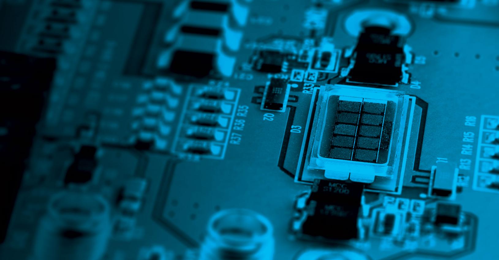
Sales of the VCSEL are rising far faster than its more common cousin, the edge-emitting laser, due to its superior attributes. Merits include its vertical architecture (see Figure 1 (a)), which simplifies production by removing the need for cleaving wafers and coating facets. After processing, all that is needed is to dice the wafer. Another feature of the VCSEL is its relatively short cavity, enabling high data rates. These strengths, plus the circular emission profile that is defined by the aperture, have made the VCSEL a very competitive and successful product for data communications, and are driving its success in 3D sensing. For the latter, higher output powers are required, realised by assembling arrays of apertures on a single die.
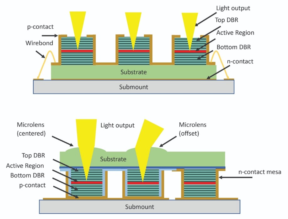
Figure 1. VCSEL designs feature a pair of distributed Bragg reflectors (DBRs). These reflectors provide the mirrors for a resonant cavity that contains the actives layers, featuring multiple quantum well structures. In a top-emitting VCSEL (a), light is emitted from the top of the wafer. This design requires wire bonds for electrical connection. In TriLumina’s novel, back-emitting VCSEL (b), light is emitted from the back side of the wafer. In this configuration, no wire bonds are required and lenses can be monolithically etched above the emitter to either reduce beam divergence (centred microlens) or shift the output angle of the beam (offset microlens). Note that the features are not to scale.
The traditional VCSEL is a ‘top-emitter’ – that is, light is emitted through the top of the semiconductor wafer. But that’s not the only possible configuration. At TriLumina of Albuquerque, NM, our team is pioneering the ‘back-emitter’, an architecture offering greater flexibility in VCSEL array design. To produce our devices, we grow the heterostructure up-side down compared to the top-emitter, and use special layers within the laser structure to realise electrical connections to the anode and cathode (see Figure 1 (b)).Our back-emitting VCSEL configuration has several notable advantages over its conventional sibling. It requires no wire bonds for electrical connections to the array – instead, the VCSEL die is simply flip-chip bonded to a sub-mount that has all of the required electrical connections defined. Thanks to the absence of wire bonds, back-emitting VCSEL die can be tiled close to one another to form large illumination modules that produce enough power for long-range sensing applications. In addition, eliminating wire bonds trims the parasitic impedance of the package, and in turn speeds rise and fall times, improving the performance for pulsed depth-sensing applications.
Another merit of back-side emission is that it allows micro-lenses to be monolithically etched directly into the emitting surface. Armed with this feature, beam shaping is possible: either reducing the divergence of each emitter, or diffusing light output. What’s more, lenses can be offset from the emitter aperture to steer the beam off-axis. This enables fully solid-state beam steering, by combining beam pointing with individual addressability of zones of the VCSEL apertures. Armed with these features, the overall system cost for 3D sensing can be reduced by eliminating optical elements or beam steering components.
What wavelength?
For engineers that design 3D sensing systems, one of their biggest decisions is the selection of the operating wavelength. Common lasing wavelengths include 850 nm, 905 nm, 940 nm and 1550 nm. The wavelength that an engineer selects will influence: eye safety; visibility, as sources that meet eye safety requirements can still be distracting; interference from ambient light; and the availability of sensors for detection. Note that all these considerations can impact other aspects of system design.
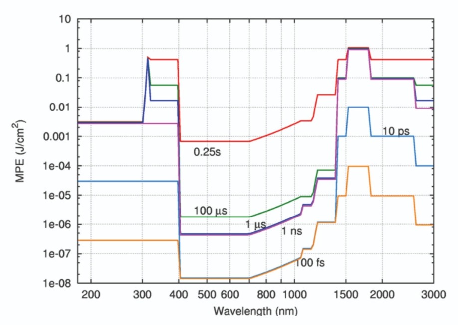
Figure 2. The maximum permissible exposure for eye safety, calculated as a function of wavelength and pulse width, for a fixed energy per pulse. For high-power point sources, eye safety configurations push systems to longer wavelengths. For VCSEL arrays, individual emitter output can be quite low, enabling eye-safe operation, even when the total array output is high.
To meet eye safety requirements, engineers must comply with the maximum permissible exposure level. This varies with wavelength and the duration of the pulse (see Figure 2). Independent of wavelength, shorter pulses have a lower maximum permissible exposure (this is a result of the way the plot, shown in Figure 2, is constructed, as the same amount of energy is being delivered in a short pulse and a long pulse). For 3D sensing systems, pulse widths can be as short as 10 ns – and even less in some cases. This increases the burden on eye safety considerations. Moving to longer wavelengths can ease this, as sources operating at 1550 nm allow for the greatest pulse power for eye safety limits.VCSEL arrays typically operate at 850 nm to 980 nm. This might suggest, based on Figure 2, that eye safety would limit output powers compared to sources at longer wavelengths. However, it’s not that simple. That’s because eye safety considerations account for the difference between an array of lower-power sources and a single, high-brightness emitter, such as an edge-emitting laser. Far from the source, VCSEL arrays appear to be a single, circular output beam, and at these distances they behave like point sources. But as one gets closer to a VCSEL array, they become an extended source and eye safety considerations change, now being determined by the output of individual emitters. That’s welcome, as it can slash the overall power factors by up to four orders of magnitude, and make 940 nm VCSEL array sources nearly equivalent to point sources at 1550 nm in regard to eye safety.
Another consideration, which affects the performance and cost of the system, is the level of background illumination at or near the source wavelength. When background illumination is high, it must be suppressed with additional filtering. To gauge the level of filtering required, one can consider the solar radiation at air mass 1.5. Data provided by NREL (see Figure 3) reveals the level of background at the wavelengths 850 nm, 940 nm, and 1550 nm. At 850 nm, radiation is relatively high, and additional filtering is required for systems operating at this wavelength. Both 940 nm, which is not coincidentally where the iPhone X VCSELs operate, and 1550 nm, have reasonably low background radiation.
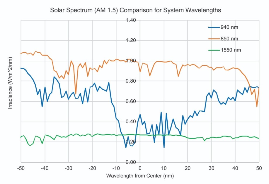
Figure 3. The AM 1.5 reference spectrum from NREL is shown centred at three different wavelengths (850 nm, 940 nm, and 1550 nm). Ambient solar light can become background noise in 3D sensing systems. To limit this background, systems can be formed at 940 nm or 1550 nm, rather than 850 nm.
One final wavelength-related consideration relates to the availability of suitable sensors. There are three different commonly available detector types used for 3D sensing systems: silicon avalanche photodiodes; multi-spectral CMOS imagers; and compound semiconductor detectors and arrays, like InGaAs avalanche photodiodes. The first two types are compatible with 850 nm and 940 nm sources, while the latter is needed for those operating at 1550 nm (see Figure 4). When cost is a concern, silicon sensors are preferred. There are a wide variety of silicon sensors with imagers supporting many different approaches to 3D sensing.Coping with the heat
All of the key markets for 3D sensing systems – consumer, industrial and automotive – require the optical source to maintain performance over an extended temperature range. The toughest requirements are found in the automotive sector, where operation may need to extend from -40 °C to +125 °C. This challenge is particularly tough because, to prevent system costs from escalating, the illumination source must ideally run without temperature control. Unfortunately, the characteristics of the laser change with temperature, including its wavelength and its output power.
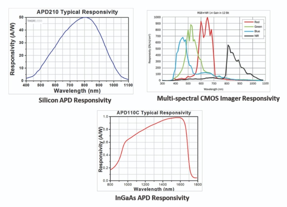
Figure 4. Responsivity, as a function of wavelength, for three different candidate sensors for 3D sensing systems. To trim system costs, silicon detectors and CMOS imagers are preferred over their more expensive III-V counterparts.
With VCSELs, changes with temperature are far smaller than those of edge-emitters, eliminating the need for temperature control for appropriately designed 3D sensing systems. Shifts in wavelength are lower by a factor of five, down from typically 0.4 nm/K to 0.07 nm/K. The superiority of wavelength stability stems from the use of far shorter cavities, which result in the resonator modes within the VCSEL being widely separated in wavelength. When the VCSEL heats up, the resonator wavelength and the gain profile shift to a longer wavelength. However, only one resonant mode overlaps the gain profile, and this determines the wavelength. In contrast, in an edge-emitter, resonator modes are narrowly separated in wavelength, so when the gain profile shifts, a new lasing mode emerges at the gain peak, leading to a new lasing wavelength.The shift in the output power of semiconductor lasers with temperature tends to be associated with the resonator mode and gain profile shifts, and changes in non-radiative recombination rates. The extent of the variation in power is strongly dependent on the design, but in a typical edge-emitter it can plummet to near zero at 85 °C. In contrast, our VCSEL arrays operate at up to 125 °C at close to 70 percent of the rated power at 25 °C (see Figure 5), meeting the most demanding automotive requirements without the need for temperature control systems.
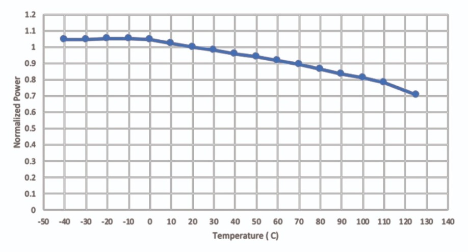
Figure 5. The output power of a TriLumina illumination module operating at 0.1 percent duty cycle (10 ns pulse, 100 kHz repetition rate), as a function of temperature. Output power is normalized to the output power at 25 °C. At 125°C, the illumination module still produces over 70 percent of its rated power.
Ensuring reliabilityReliability is a key concern, especially in automotive applications where user safety is critical. Our VCSELs excel in tests to judge this characteristic, because the back-emitting architecture is inherently robust to the typical stresses used for assessing reliability. The n- and p- contacts sit on the same side of the VCSEL array, and are both entirely clad in metal or silicon nitride. Thanks to this design, there are no ingress paths for moisture into the active area of the device.
That’s not the case for the top-emitting VCSEL, which needs to have an opening in the p- contact to allow light to exit the device. It is only fair to point out that these top-emitting VCSELs have been shown to be highly-reliable – but we have no doubt that our back-emitting configuration provides even greater confidence for long-term operation. We find no evidence of degradation when driving our arrays under accelerated conditions for over 9,000 hours. We are now undertaking full evaluation of our 8 W illumination module to the automotive quality standard, AEC-Q102, and expect to complete qualification before this article is published.
Expanding the range
Depth-sensing systems use various approaches to determine distance. For short-range systems, either a structured light approach is adopted, such as in the iPhone X, or one based on stereoscopic vision. For medium to long-range systems, including LiDAR, the more common approaches are based time-of-flight. They can be either direct, using a flash; or indirect (see Figure 6).
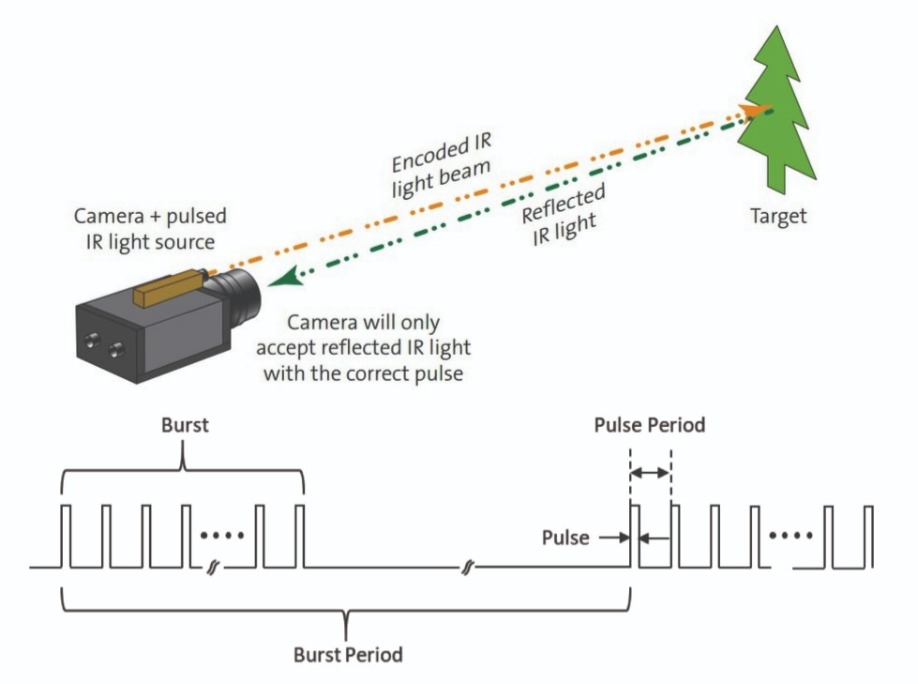
Figure 6. In a differential time-of-flight system, a pulsed infrared source illuminates an object with an encoded (pulsed) beam. The arrival time of the reflected pulse is measured with a detector or a camera system. The encoding scheme tends to employ a burst pattern, repeated at a burst period that corresponds to the maximum measurement range of the system. A notional burst pattern, shown here, can contain additional pulse patterns that allow the system to disambiguate multiple reflections, or other spurious returns.
We have designed and delivered back-emitting VCSEL array modules to customers covering every range, from consumer applications requiring depth sensing over a few metres to front-facing automotive LiDAR operating at 250 m or more (see Figure 7 for examples of our products, and Table 1 for key metrics for the illumination modules).Our lasers are going into short-range systems, providing a key ingredient in world-facing cameras for mobile applications. The unique advantage of illumination modules formed with our VCSELs is that they can be soldered directly to a printed circuit board, like any other electrical component. This makes them a low-cost option for replacing LEDs with VCSEL sources. Modules run at low duty cycles – typically a 1 percent to 3 percent average duty cycle – and they produce an output power of about 4 W.
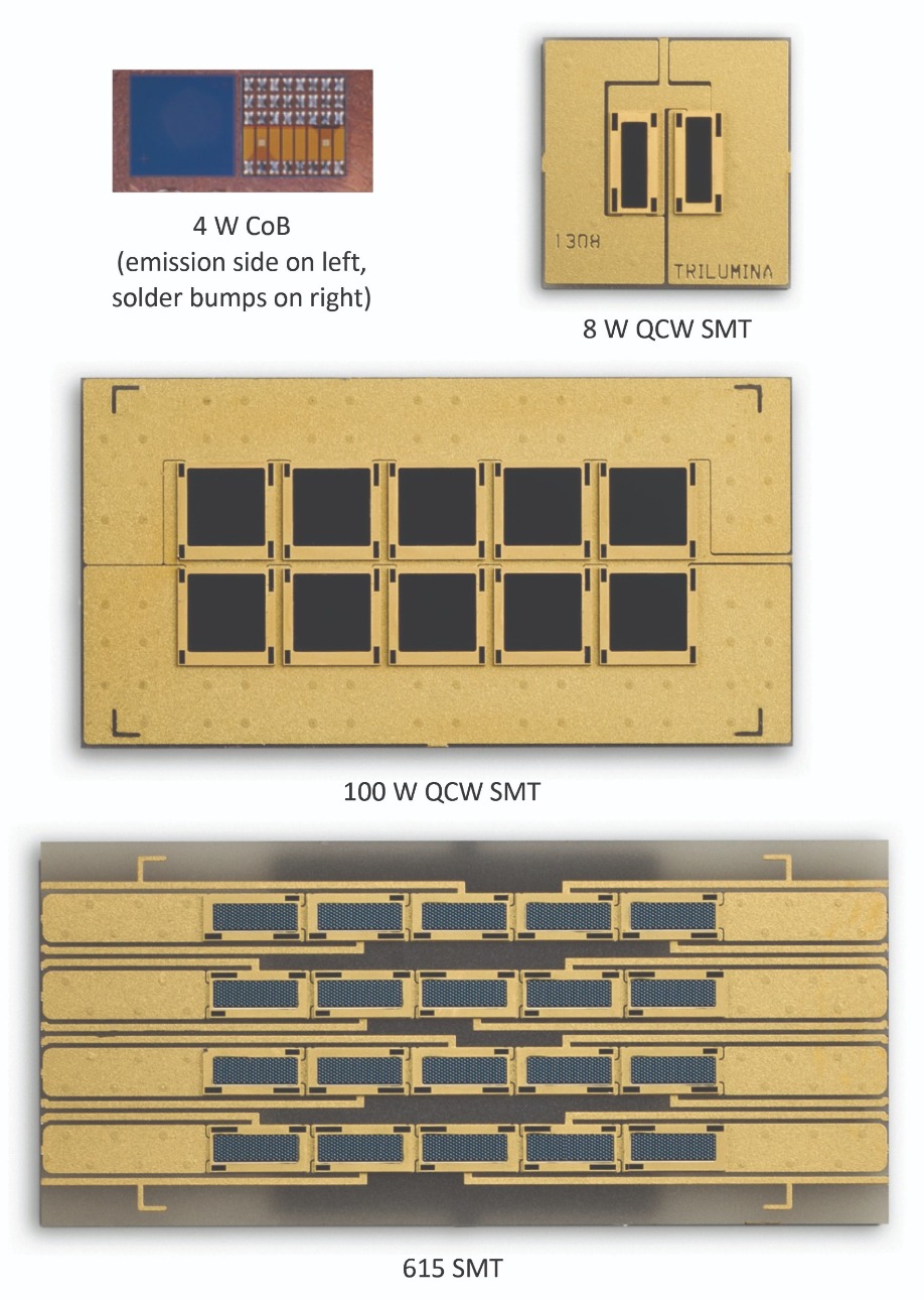
Figure 7. Examples of TriLumina’s illumination modules, for ranges from 5 m to 300 m.
Offering a little more power are our illumination modules that target automotive safety applications, such as occupant monitoring. Examples include two 1 mm x 2 mm die that are connected in series, mounted onto a ceramic sub-mount, and produce an output of around 8 W at a 3 percent duty cycle.For the 50 m to 100 m range, our illumination modules are being deployed in multi-mode time-of-flight cameras. These are used in indirect time-of-flight systems, featuring multi-spectral CMOS imagers that attain high-resolution depth maps, along with black-and-white and infrared images. The cameras are positioned at the four lamp locations on an automobile and enable the driver to benefit from increased awareness and safety. For this application, we produce 100 W modules, operating at a 2 percent duty cycle, formed from ten 2 mm x 2 mm VCSEL arrays on a ceramic sub-mount.
We ship 600 W illumination modules for the longest ranges. Assembled from twenty 1 mm x 2 mm die, and housed on a ceramic sub-mount, they are suitable for direct time-of-flight and flash front-facing LiDAR systems. To realise a narrow divergence – it is approximately 12 degrees, in terms of its full-width at half maximum – micro-lenses are etched into the chip. Using pulses as short as 10 ns or so, delivered at a 100 kHz repetition rate, LiDAR realises the specified range. Note that it is the low duty cycle of just 0.1 percent that allows the module to hit its high peak power.
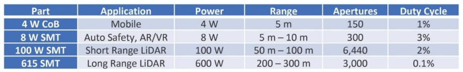
Table 1. TriLumina illumination modules by range and application.
They key to the competitive performance of all our modules is our unique back-emitting VCSEL array design. Often, to develop a new module, all we need to do is to produce a new ceramic sub-mount design. By tiling our VCSEL array die in appropriate series or parallel networks, or sometimes a combination of the two, we can fulfil the desired electrical and optical specifications.Looking ahead
VCSEL technology is continuing to make its way into new applications. The advent of the 3D sensing system has made the VCSEL array a very strong contender for infrared illumination. Armed with our back-emitting laser with integrated microlenses, we are able to offer a compelling product that helps to drive down the total system cost for advanced 3D sensing systems. The back-emitting configuration paves the way for higher levels of integration that will see VCSEL technology used in innovative designs at the forefront of 3D sensing.


