
Solving the mystery of quantum light in thin layers
A very special kind of light is emitted by WSe2 layers, according to Austrian scientists
It is an exotic phenomenon that nobody was able to explain for years: when energy is supplied to a thin layer of the material WSe2, it begins to glow in a highly unusual fashion. In addition to ordinary light, WSe2 also produces a special type of bright quantum light, created only at specific points of the material. It consists of a series of photons that are always emitted one-by-one - never in pairs or in bunches.
This anti-bunching effect is perfect for experiments in the field of quantum information and quantum cryptography, where single photons are required. However, for years this emission has remained a mystery.
At the Technical University of Vienna an explanation has now been found: A subtle interaction of single atomic defects in the material and mechanical strain is responsible for this quantum light effect. Computer simulations show how the electrons are driven to specific places in the material, where they are captured by a defect, lose energy and emit a photon. The solution to the quantum light puzzle has now been published in the journal Physical Review Letters.
WSe2 is a 2D material that forms extremely thin layers only three atomic layers thick: there are tungsten atoms in the middle, coupled to selenium atoms below and above. "If energy is supplied to the layer, for example by applying an electrical voltage or by irradiating it with light of a suitable wavelength, it begins to shine," explains Lukas Linhart from the Institute of Theoretical Physics at the TU Vienna. "This in itself is not unusual, many materials do that. However, when the light emitted by WSe2 was analysed in detail, in addition to ordinary light a special type of light with very unusual properties was detected."
This special nature quantum light consists of photons of specific wavelengths - and they are always emitted individually. It never happens that two photons of the same wavelength are detected at the same time. "This tells us that these photons cannot be produced randomly in the material, but that there must be certain points in the WSe2 sample that produce many of these photons, one after the other", explains Prof. Florian Libisch, spokesperson of the Graduate School TU-D at the TU Vienna with a focus on 2D materials.
Explaining this effect requires the detailed understanding of the behaviour of the electrons in the material on a quantum physical level. Electrons in WSe2 can occupy different energy states. If an electron changes from a state of high energy to a state of lower energy, a photon is emitted. However, this jump to a lower energy is not always allowed: The electron has to adhere to certain laws - the conservation of momentum and angular momentum.
Defects and distortions
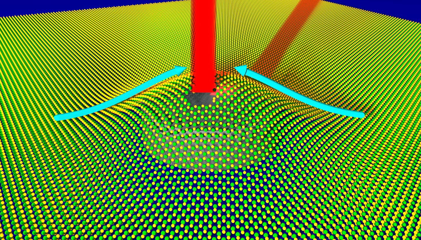
Due to these conservation laws, an electron in a high energy quantum state must remain there - unless certain imperfections in the material allow the energy states to change. "A WSe2 layer is never perfect. In some places one or more selenium atoms may be missing," says Lukas Linhart. "This also changes the energy of the electron states in this region."
Moreover, the material layer is not a perfect plane. Like a blanket that wrinkles when spread over a pillow, WSe2 stretches locally when the material layer is suspended on small support structures. These mechanical stresses also have an effect on the electronic energy states.
"The interaction of material defects and local strains is complicated. However, we have now succeeded in simulating both effects on a computer" says Lukas Linhart. "And it turns out that only the combination of these effects can explain the strange light effects." At those microscopic regions of the material, where defects and surface strains appear together, the energy levels of the electrons change from a high to a low energy state and emit a photon. The laws of quantum physics do not allow two electrons to be in exactly the same state at the same time, and therefore the electrons must undergo this process one by one. This leads to the photons being emitted one by one as well.
At the same time, the mechanical distortion of the material helps to accumulate a large number of electrons in the vicinity of the defect, so that another electron is readily available to step in after the last one has changed its state and emitted a photon.
This result illustrates that ultrathin 2D materials open up completely new possibilities for materials science.


