

Single-wafer processing streamlines SiC production
Replacing batch lapping and polishing with a single-wafer grind and polish enables scalability in SiC substrate production while improving consistency, increasing yield and lowering the manufacturing cost
BY ROBERT RHOADES FROM REVASUM
SiC is renowned for being difficult to grow and process. Falling just below diamond on the Mohs hardness scale, it is chemically inert to all but the most aggressive etchants. Such traits make SiC a challenging material to produce. However, it is well worth the effort, because this wide bandgap semiconductor can make great devices. Following several decades of development, commercial SiC diodes and transistors are combining high voltages with high powers and high frequencies to outperform those made from silicon by a substantial margin. Sales are now rising fast, with demand outpacing supply, as devices are deployed in the automotive, IoT, power regulation, and 5G markets (see box “The primary opportunities for SiC devices” for details).
Growth in just one of these market segments will justify the expansion of SiC wafer production capacity over the next five to ten years. So, when ramping demand from all these sectors is taken into account, one can see that there is a tremendous opportunity for makers of SiC material.
The leading supplier of SiC substrates, US firm Cree, recently announced plans to increase its production by a factor of 30 over the next few years. Others are sure to follow suit and announce their own plans soon. However, for all these companies, cranking up SiC substrate production cannot be done by simply flicking a switch. Ramping capacity is constrained by the time taken to build and qualify furnaces – even for experienced teams, this can take a year or more to bring on line. For companies just getting into SiC production, the time that this will take will surely be much longer, given that the growth conditions necessary to achieve the best quality single-crystal SiC – such as the optimum times, temperatures, and flow rates – are trade secrets. When all these factors and difficulties are accounted for, some sources estimate that demand will exceed capacity to at least 2030.
Given the high level of demand for SiC substrates, to ensure that this industry has as much success as possible, it is essential to manufacture these wafers in the most efficient manner. Traditionally, they have been produced with batch processes, but there is an alternative, offering better consistency, higher yields, and a lower cost of manufacturing: single-wafer processing. At Revasum of San Luis Obispo, we are pioneering the production of equipment that is dedicated to this approach.
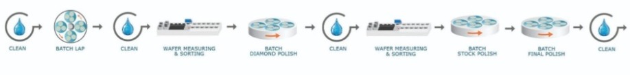
Figure 1. A typical batch processing sequence requires six process tools: a lapper, diamond polisher, stock polisher, fine polisher, standalone cleaner and a wafer sorter.
Batch processesThe historical, batch-based process for making SiC wafers, illustrated in Figure 1, begins by growing a boule and sawing or slicing it into individual wafers. They are then loaded into a batch lapping system to remove slicing damage, reduce thickness, and make the top and bottom surfaces parallel. After manual unloading and cleaning, wafers are measured and sorted into groups by thickness, generally using a large sorting system.
The sorting process is necessary to match thicknesses within a batch as tightly as possible, because it enables the use of a reasonably uniform pressure distribution during the batch polish process. If sorting were not undertaken, the batch polish process would remove more material from thicker wafers, and less material from thinner wafers. For the latter, some of the damage could remain, requiring them to be reworked.
After sorting, a batch polish takes place, using a diamond abrasive to remove lapping damage and provide a lower surface roughness. This is referred to as a diamond polish. Wafers are then unloaded and cleaned once more before going to a different batch polisher for the stock polish step, using a different pad and slurry.
Following the stock polish, wafers are unloaded, cleaned, and reloaded into yet another batch polisher – with a different pad and slurry – for the final step polish, which removes only a small amount of material, typically less than 0.5 µm. The purpose is to realise the final surface finish required for epigrowth.
Figure 2. A typical single-wafer processing sequence requires a grinder and a polisher, each with an integrated cleaning module.
In the stock and final polish steps, the total amount of material that’s typically removed varies from 1.5 µm to 3.0 µm. The exact value is governed by the diamond size used in the previous step.Following this, wafers are unloaded manually one more time, and taken to a cleaning system, where they are measured and inspected. This determines which wafers need to be reworked. Due to wide variations within each batch, it is not uncommon for a significant percentage of wafers to be reworked. In some cases 40 percent of the wafers have to go through a second set of stock and final polish steps.
Reworking is by no means the only drawback associated with batch processing. It is notoriously messy, and there is a substantial risk that wafers are dropped while attempting to load and unload with gloved hands. Another issue is that it takes time to safely unload wafers into a wet storage tank at the end of the cycle. Consequently, some of the wafers can dry out, and are left with particles and debris on their surface. These contaminants are difficult to remove and can be the cause of a major loss in yield.
The number of wafers processed in a batch depends on their size, and typically varies from 16 to 28. By processing this many at one time, a relatively high net throughput results, even with long process times for SiC. The rub, though, is that all of the wafers in the batch are simultaneously at risk. Crack or break just one of them during the process and it is virtually impossible to stop the machine fast enough to prevent all of the other wafers in the same batch from being destroyed. Since SiC wafers command a high unit price – reportedly it’s up to $2000 per wafer – loosing an entire batch can be extremely expensive.
Finally, as the SiC industry moves to larger wafer sizes, the net throughput advantage of batch processing diminishes. That’s because fewer and fewer wafers will fit within the fixed platen surface area of any given tool. For example, a typical batch tool that holds 30 wafers with a diameter of 100 mm wafers can only accommodate a dozen 150 mm wafers, and just nine 200 mm wafers. Note that 100 mm SiC production is already well established, 150 mm production ramping fast and 200 mm development underway, so the greatest asset of the batch approach – parallel processing of many wafers – is being rapidly eroded.
The single-wafer solution
The single-wafer process that we advocate has the same starting steps of boule growth and slicing (the full sequence of steps is illustrated in Figure 2). After this, wafers are loaded into an automated wafer grinder. Options include the Revasum 7AF-HMG, a hard materials grinder made by our team. It begins by grinding one side of a wafer to a target thickness with a two-step sequence. After this, the wafer is cleaned and flipped, ground in another two-step sequence on the other side to a lower target thickness, and then cleaned and unloaded without human touch.
To maintain accuracy and control, the 7AF-HMG is equipped with in-situ thickness probes that monitor wafer thickness during each grind step. This helps to ensure a good thickness consistency. Wafer-to-wafer thickness variation is less than 1 µm, enabling the sampled measurement data for quality control to often be sufficient as opposed to requiring data from every wafer for sorting in a batch approach. So long as the appropriate fine grind wheel is utilised, the surface roughness and the depth of damage are low and well controlled.
Using this approach removes the need for a diamond step-down polish and also the requirement for measuring and sorting into groups. Instead, all wafers are directly loaded into a wafer polisher. In addition, the amount of total removal for stock and final polish is just 1.5 µm.
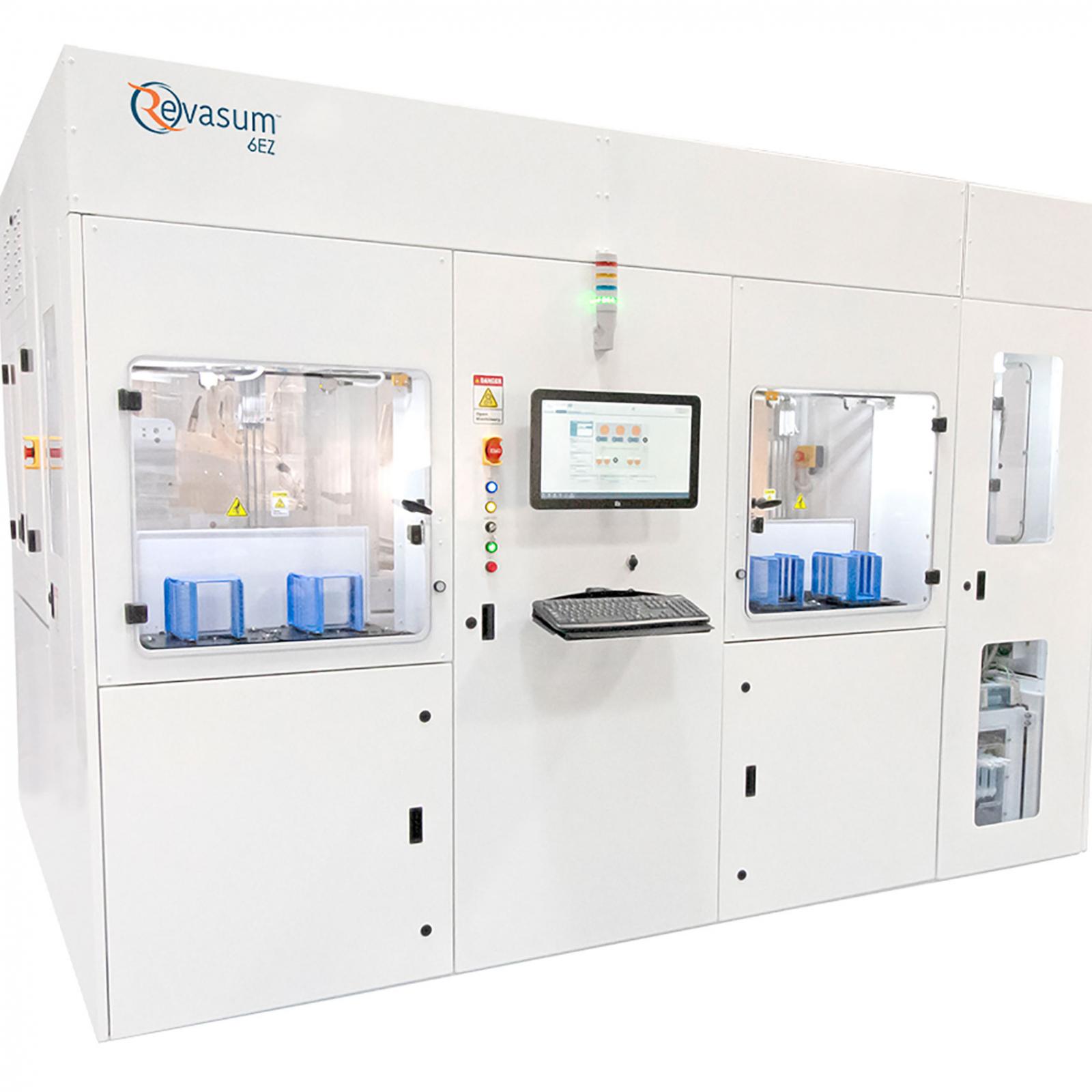
Offering this capability is our 6EZ automated wafer polisher. Released this October, it is the first fully-automated, single-wafer polisher designed specifically for SiC substrates. It is capable of polishing and cleaning both faces of 50 SiC substrates sequentially, without any operator intervention.
Customers that use our 6EZ usually begin with a three-step polish on one side of a SiC wafer. After this the wafer is flipped and an integrated clean applied, before a three-step polish proceeds on the other side of the wafer, followed by another wafer flip, a second integrated clean, and finally an unload. For all these steps, fully automated wafer handling takes place, along with single-wafer control. An overhead diagram of the 6EZ, illustrating where the various steps take place, is shown in Figure 3.
The first significant advantage of single-wafer processing is that it reduces the total number of tools in the process sequence. Benefits that result include a simplification of procedures, and a reduction in the total floor space required for any given production level. Rather than requiring six process tools for batch processing of SiC – a lapper, diamond polisher, stock polisher, fine polisher, separate cleaner, and a wafer sorter – all that’s needed is a grinder and a three-step polisher, each having integrated cleans.
What’s more, there is no longer a need for a wafer sorter. That’s partly because the grind process is very consistent. It is also a result of independent control of the polish steps for each wafer, reducing sensitivity to differences in wafer thickness. Yet another advantage is that it may be possible to use fewer metrology tools, as there is no longer the need to measure every wafer at multiple steps just so they can be sorted.
A second strength of single-wafer processing is that it can slash the number of labour hours needed to support any given production volume. There are many reasons behind this: there are fewer operations in the overall process sequence, the manual loading and unloading for each batch tool is eliminated, there is no longer the need to sort wafers into different batches, and there is less need for in-line data measurements.
The third set of advantages relate to consistency and control. By their very nature, fully automated single-wafer tools are designed to provide each wafer with the same process conditions. No longer are there concerns that wafers within a batch are having an impact on one another. Using well designed control systems and feedback mechanisms, it is possible to ensure that the physical conditions are the same from run to run.
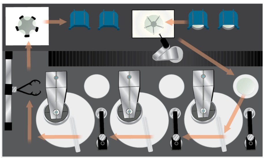
Figure 3. An overhead shot of Revasum’s 6EZ, the first fully-automated, single-wafer polisher designed specifically for SiC substrates.
In our case, this is realised by carefully considering every possible impact that our tools have on the process, from the grind wheel feed rates and speeds on the 7AF-HMG to the polish downforce and table speeds on the 6EZ. Fabs that invest in our tools can be confident that every wafer is individually processed with the same recipe settings and experiences the same process conditions. This results in higher productivity (less rework) of higher quality wafers.On top of these three key advantages, there is another that is easy to overlook. With single-wafer processing, there is much merit in scaling to larger wafers, the direction the industry is heading. Since wafers are processed one at a time, the net throughput is essentially independent of wafer size. In sharp contrast, with batch processing net throughput is tied to the number of wafers per batch, and this is a strong function of wafer size. Batch processes that are efficient and cost effective with 100 mm wafers are less efficient and more costly as the size of the wafer increases.
The final, and possibly most important advantage of single-wafer processing is that it produces a higher yield. With each wafer processed individually, excellent consistency is maintained wafer after wafer, day after day. So long as grind and polish processes are optimised properly, the in-line process yields should average well over 95 percent, maximising productivity and driving down costs. Of course, many other factors beyond grind and polish will contribute to overall yield, but the goal, at each unit process, is always to maximize yield, while minimising the risk of broken wafers.
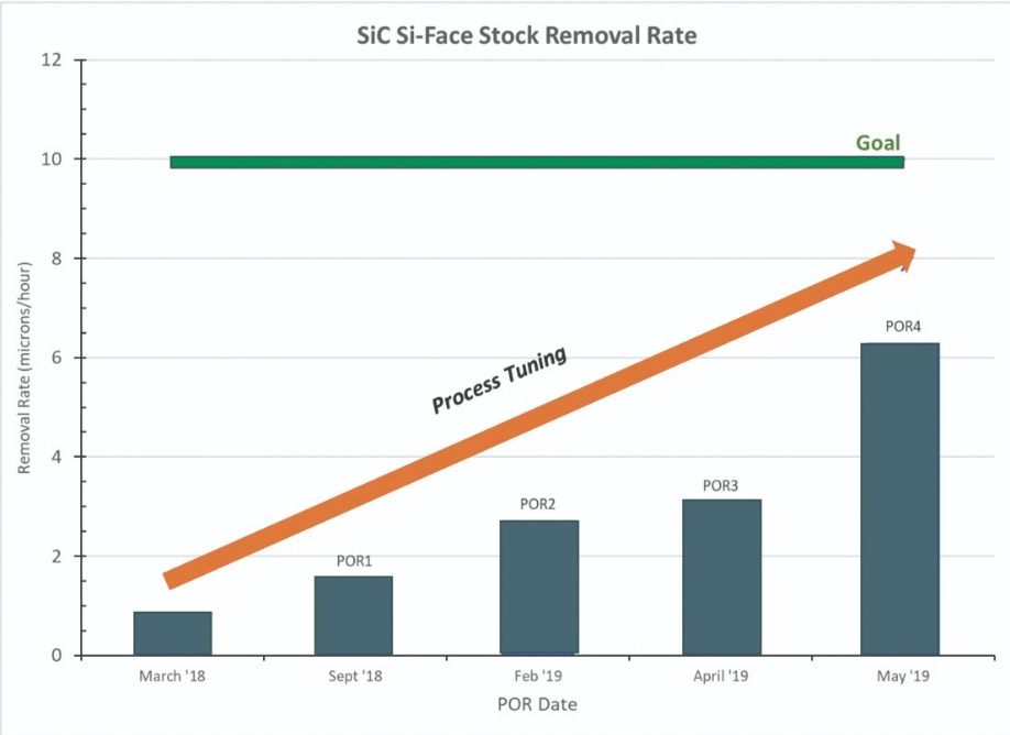
Figure 4.Rate graph (showing goal of 10 µm/hr)
With demand for SiC strong, and widely expected to grow over the next decade and beyond, there needs to be a massive ramp in SiC capacity alongside improvements in the wafer manufacturing processes that will increase yield and lower cost. One great opportunity for improvement is the transition from batch lapping and polishing to single-wafer grind and polish. The new generation of tools currently coming to market, such as those released by our team, offer scalability to 200 mm wafer sizes alongside greater consistency, higher yields, and a lower cost of manufacturing.One of the most significant drivers behind the increasing demand for SiC devices is the rising production of electric vehicles. Over the next ten years, nearly all major car manufacturers are planning to shift a significant portion of their production from vehicles with internal combustion engines to those that run on electricity. Sales of electric vehicles are projected to grow from a current level of $2-3 billion to roughly $16 billion by 2030. One of the gating items for this growth is the availability of SiC components for the power conversion modules.
The second broad segment that is driving demand for SiC is power devices and voltage regulation. This sector includes discrete power devices and power regulation modules, serving everything from computer data storage farms to systems for the efficient harvesting of alternative energy sources, such as solar grids and wind turbines. For many of these applications, SiC is selected primarily for its power efficiency, which stems more from the low-loss properties of this semiconductor, rather than its high-voltage capability. Compared to silicon-based voltage regulating power supplies for data storage systems, those made from SiC components are about 30 percent more efficient. This leads to two simultaneous savings: less electrical power required to run the system; and the SiC chips generate less heat, trimming the load on the air conditioning system that cools the room.
The third major market where SiC is destined to make an impact is 5G mobile communications equipment. Here, devices will be used to satisfy power and high-frequency demands. One of the drawbacks of moving to the higher operating frequencies of 5G networks is that signals suffer from stronger attenuation in the atmosphere. To address this, there will be more base stations spaced more closely together – now they typically cover only one city block. These base stations will have to handle more signals and more data packets than ever before, so they will have to operate at higher power levels. Due to these requirements, SiC is being designed into the power regulation and driver circuits. While the majority of the RF signals generated at 5G base stations will come from GaN HEMTs, due to a lack of native substrates, these devices are grown on SiC, creating yet another growing market for this substrate.


