

Empowering power electronics with PowerAmerica

PowerAmerica targets the primary obstacles to widespread adoption of wide bandgap power electronics: high costs, concerns with reliability and ruggedness, and a lack of expertise in the workforce.
BY Victor Veliadis FROM POWERAMERICA
There are several reasons behind silicon’s dominance of the power electronics market. Silicon is renowned for its excellent starting material quality, its ease of processing, the opportunity for low-cost mass production, and proven reliability. However, despite significant progress, silicon devices are now approaching their operational limits. They are held back by their relatively low bandgap and low critical electric field, traits that result in high conduction and switching losses and a substandard high-temperature performance.
To address these shortcomings, much effort is being directed at increasing the competitiveness of commercial SiC and GaN power devices. Transistors and diodes made with these wider bandgap semiconductors have superior material properties, enabling the production of highly efficient power devices with a smaller form factor and reduced cooling requirements.
Helping to exploit the potential for energy saving and technological innovation are several initiatives promoting the adoption of these wide bandgap power devices. In the US, a number of government programmes have already played a major role in supporting early work to develop advanced crystal growth of SiC and GaN, wafer fabrication and device processing technologies. As far back as the late 1980s, organizations such as the Air Force Research Laboratory, the Army Research Laboratory, the Office of Naval Research, the Missile Defense Agency, and the Defense Advanced Research Projects Agency provided hundreds of millions of dollars to fund what has been decades of work at universities, industry, and government laboratories. Efforts initially focused on developing critical enabling technologies such as high-quality substrates and epitaxy; and unit process steps such as ion-implantation, implant activation and gate oxidation. Success ensured a domestic source for the US Department of Defense Wide Bandgap systems.

Many of the students trained in hands-on PowerAmerica projects will go on to staff Universities or enter the industrial workforce. This will accelerate wide bandgap technology innovation.
More recently, the Advanced Manufacturing Office of the US Department of Energy and North Carolina State University have formed PowerAmerica, a National Network for Manufacturing Innovation Institute. This initiative, which commenced in 2015 and has a five-year budget of $150 million, is directed at improving cost-effective, large-scale production of wide bandgap power electronics. Efforts are aimed at addressing manufacturing gaps in wide bandgap power technology. Success will enable high-tech job creation, technological innovation, and a hike in the energy efficiency associated with many different applications.
Overcoming barriers to adoption
Today there is no question that wide bandgap devices are well beyond the stage of proof-of-concept. For example, it’s been nearly two decades since Infineon launched the world’s first commercial SiC Schottky diode. However, commercial progress has been slow, primarily due to three factors. One is that costs are far higher than those for mass-produced silicon, chiefly because manufacturing volumes are low and the dedicated foundries used for GaN and SiC production are not fully loaded. A second significant issue is that there are ruggedness and long-term reliability concerns. And the third issue is that the workforce lacks expertise in integrating wide bandgap technologies into systems – like many industries, the power electronics industry is traditionally slow to change and adapt to new technologies.
To tackle all these three issues, PowerAmerica is running over 35 industrial, university, and national laboratory projects annually. Projects are scheduled to complete their scope of work in a single year. This programme of activities will enable US leadership in wide bandgap power electronics manufacturing, work force development, job creation, and energy savings.
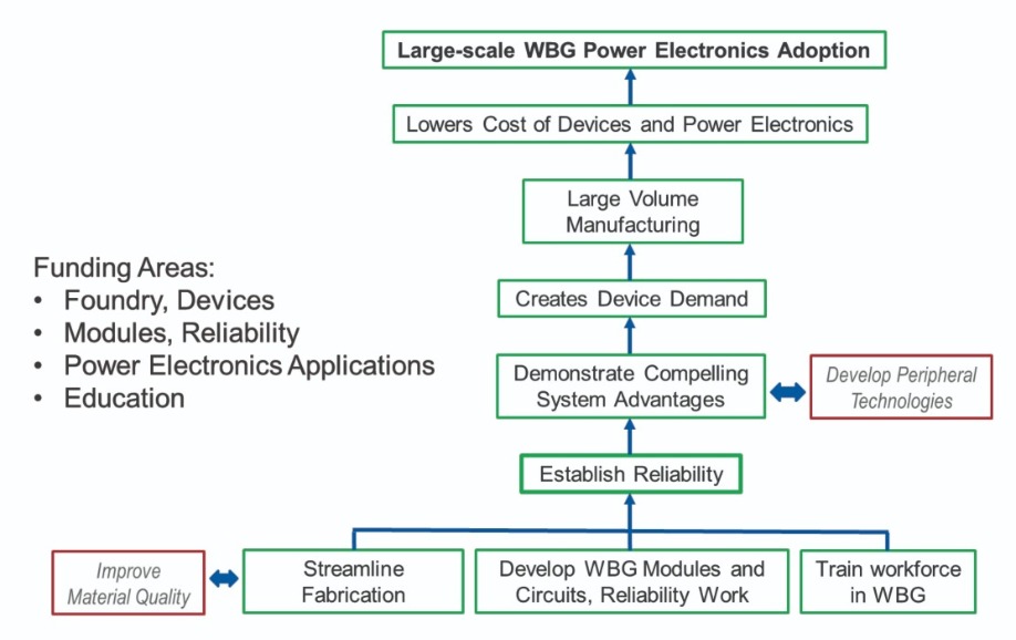
Figure 1. PowerAmerica funds projects in areas that synergistically culminate in large-scale wide bandgap power electronics adoption (green boxes). The red boxes represent key technology areas that are presently outside the Department of Energy PowerAmerica mission.
Cutting costsThe efforts of PowerAmerica are taking place against a backdrop of falling prices for wide bandgap power devices. During the last eight years, prices of commercially available SiC MOSFETs have plummeted by about 80 percent, thanks to a combination of an increase in manufacturing volume, technological innovation, and an a move to larger-area wafers – 150 mm is now the common diameter. However, the prices of wide bandgap devices are still about three-to-four times higher than those of similarly rated components made from silicon.
One way to trim costs is to exploit economies of scale. This can be accomplished by repurposing 150 mm and 200 mm silicon foundries. If these foundries have not kept pace with the channel length reductions of the last two decades, this opportunity may have great appeal. That’s because it allows the lines to manufacture legacy silicon parts while ramping up SiC fabrication, which requires relatively modest 0.5 µm design rules. Although investment will be needed to support fabrication steps that are unique to the production of wide bandgap devices, such as high-temperature implantation and annealing, contact formation, and backside processing, a capital investment of $12 million to $15 million should be sufficient.
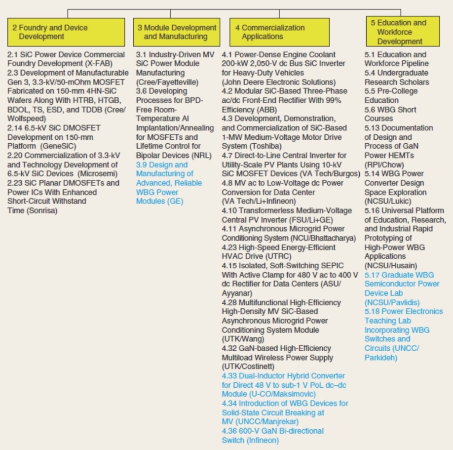
Figure 2. Strategic PowerAmerica 2018-2019 budget period projects synergistically accelerate commercialization of wide bandgap power electronics. New member projects are shown in blue font.
Taking this approach lowers both material and process costs, so long as the foundry is loaded close to capacity with silicon and SiC wafers running on the same line – and that standard, high-yield SiC process blocks are offered for the majority of SiC fabrication, to ensure mass production. Note that today the latter is challenging, as SiC ‘device’ companies tend to compete on design as well as process integration, an area where many hold extensive IP portfolios.Pioneering this approach is the collaboration between PowerAmerica and X-FAB, which is a facility that has 150 mm SiC wafers fully integrated within a high-volume, automotive-qualified silicon foundry. In X-FAB’s lines, processing is dominated by fixed overhead costs, with the economy of scale of silicon fabrication brought to SiC manufacturing, slashing costs. Members of PowerAmerica that are fabricating at X-FAB include ABB, GeneSiC, Microchip, Monolith, UnitedSiC, Global Power, Sonrisa, The State University of New York, and North Carolina State University. In addition, several other companies are fabricating at X-FAB including many from Europe and Asia.
Costs should continue to fall with the introduction of 200 mm wafers. Thanks to this, it should be possible to produce devices for a cost that is just 50 percent more than it is for silicon, so long as the right approach is adopted in the foundry. Note that device cost is only one element of the system’s bill of materials, and that the move to wide bandgap devices reduces the demands on other components, opening the door to the production of systems that are smaller, lighter and cheaper to make.
After wide bandgap chips are produced they need to be packaged and put into modules. There are no volume manufacturing efforts in these two critical tasks in the US, because, since as far back as 1970s, semiconductor assembly and packaging has been off-shored. Complicating matters, if a GaN or a SiC chip is housed in a standard silicon module, it will fail to reach its full potential.
But it’s not all doom and gloom. The reality is that wide bandgap devices offer a unique opportunity for industrial growth, because they require modules with reduced parasitic inductance, a lower thermal impedance, higher-voltage isolation, and a higher-temperature capability. To usher in this era, PowerAmerica is funding the development of wide bandgap modules that will excel on all these fronts. They will feature specialised layouts that minimise parasitics; they will utilise new base-plate materials that will lower thermal impedance and allow for double-sided cooling; they will feature a low inductance; and they will employ new potting compounds for higher-temperature operation.

PowerAmerica applications projects, like Fast EV charger, highlight the competitive advantages of SiC and GaN devices in power electronics systems spurring further development and growth.
Ruggedness and reliabilityThe second criterion for ensuring widespread adoption, as well as improved performance, is to produce wide bandgap devices that are more reliable and rugged. Reliability can increase through improvements in material quality and fabrication. Many makers of SiC and GaN devices are now releasing their reliability data. Results indicate that performance is rivalling that of silicon. There is also a move towards greater rigour, with several industry-led semiconductor engineering trade organisations and standardisation bodies working towards the establishment of standards for these classes of power device.
Increasing the ruggedness of a power device is not easy. In practice, it requires careful consideration of design trade-offs. Ultimately, power electronics engineers have to define safe-operating-area requirements for particular applications. The chances of commercial success are much higher if the ruggedness of the wide bandgap device mimics that of silicon, since this holds the key to quick adoption.
Numerous device reliability and qualification projects have been funded by PowerAmerica (see Figure 2 for a list of projects carried out in the 2018-2019 budget period). This has led to several product releases in the marketplace. Device ruggedness projects have identified failure mechanisms and safe operating areas, and elucidated design trade-offs for optimising resistance for given ruggedness requirements. Another important initiative by PowerAmerica is the funding of the establishment of an honest broker ruggedness/reliability testing centre. The work that is done there builds ‘independent’ confidence for the suitability of wide bandgap devices in power electronics systems.
The applications projects that are supported by PowerAmerica are highlighting the compelling advantages of SiC and GaN devices in power electronics systems, including a trimming of the weight of the unit, a reduction in its volume, a higher efficiency, and a reduced bill of materials. There has also been a great deal of technological innovation, including new circuit topologies, novel gate drivers for faster switching and protection, and printed circuit board layouts that minimise inductance and eliminate ringing. These advances help to build the value proposition provided by wide bandgap electronics in the likes of laptop adapters, photovoltaic inverters, uninterruptible power systems, data centres, electric vehicle fast chargers and on-board chargers, solid-state circuit breakers, microgrid power conditioning systems, medium-voltage variable speed drives, traction inverters, and auxiliary power converters. Thanks to these successes, those in upper management are left in no doubt of the competitive advantages of wide bandgap technology. This can unlock internal funding, leading to further development.
Educating the workforce
A highly skilled workforce is the third essential ingredient to creating a substantial demand for wide bandgap devices. To realise this, during the first four years of the PowerAmerica initiative, more than $24 million of funding was used to support 63 hands-on University projects. This has equipped over 300 students with real-world wide bandgap power electronics experience.

Member-only PowerAmerica meetings provide opportunities for networking and partnerships. They also allow members to deliver a collective, amplified voice on issues that affect the wide bandgap industry, influencing its direction and shaping its growth.
During the next few years, these efforts will start to bear much fruit. Some of these students will enter the industrial workforce and help to accelerate the insertion of wide bandgap technologies into products. For those making that transition, entering the workforce has been aided by the university-industry collaborative nature of these projects. There have been ample internship opportunities, with PowerAmerica university-affiliated students spending time at ABB, John Deere, GE, Lockheed Martin, Raytheon, Eaton, Schneider Electric, XFAB, UnitedSiC, and GeneSiC. In addition, there has been a steady flow of qualified personnel taking up highly specialised wide bandgap employment positions.Other students involved in PowerAmerica will become faculty members at universities. This is also beneficial to the future of SiC and GaN, as it will help to train a new generation of students, and create a snowball effect in wide bandgap education.
To train the existing workforce, every year PowerAmerica organizes an industry-driven short course on wide bandgap semiconductors. Taught by experts from across the United States, it lasts two-and-a-half days. It is typically offered to sold-out audiences in the fall of each year. The programme is designed to provide diverse applied training, filling industry knowledge gaps, with content formulated by evaluating data from industry-wide polls asking the critical question: What training is needed to catalyse your wide bandgap growth and is not available in present educational settings? The content for this course continues to evolve, with improvements driven by attendee feedback.
Additional educational initiatives run by PowerAmerica include free, available-to-all monthly technical webinars, delivered by member experts. There are also: wide bandgap lectures, being added to power electronics courses across all 18 member universities; and tutorials offered at the winter and summer PowerAmerica member meetings, which provide an informal setting for learning and networking. Finally, to educate participants and promote the PowerAmerica wide bandgap ecosystem, I have recently delivered numerous, well-attended tutorials at mainstream trade conferences. They include the Applied Power Electronics Conference and Exposition, the International Symposium on Power Semiconductor Devices, both the International Conference on Silicon Carbide and Related Materials and its European counterpart, the Workshop on Wide Bandgap Power Devices and Applications, and the Energy Conversion Congress and Exposition. At all these gatherings there has been a recent surge in interest in wide bandgap devices.
PowerAmerica is clearly playing an important role in addressing the three key barriers to widespread commercialisation of wide bandgap power electronics: the high cost, the concerns over reliability, and the lack of expertise in systems integration of these devices. Thanks to the funding of building-block projects in device and foundry, reliability and modules, and commercial applications that synergistically culminate in large-scale wide bandgap adoption, sales of SiC and GaN devices are sure to climb over the next decade and beyond.
Victor Veliadis is greatly indebted to his team, and the Department of Energy Technical Manager Dr. Allen Hefner for his valuable technical contributions and generous support.
There are compelling incentives for membership in PowerAmerica, a 49-member institute that includes those from all areas of the GaN and SiC supply chain. One of the benefits is assistance with device design and cost-effective manufacturing in high-volume foundries. To bolster confidence in the use of SiC and GaN devices and modules in power electronics applications, support is given to ‘honest broker’ third party reliability/ruggedness evaluation centres.
Another initiative of PowerAmerica has been the establishment of a device/module bank to increase the availability and timely accessibility of long lead-time, pre-production engineering samples for power application development. By turning to the device bank, just a few days are needed for members to procure long lead-time engineering samples. That’s a great asset, as it speeds members’ development of next-generation products, while producing valuable user performance feedback that can guide manufacturer device optimisation.
One of the strengths of PowerAmerica is that it has the reach and depth to connect companies and practitioners across the wide bandgap supply chain. It provides its members with unparalleled opportunities to effortlessly make connections, create partnerships, advance technology innovation, grow their business, and build their brand. Members have complimentary access to online members-only business and technical content – including market research and presentations – and this provides powerful context and data for making sound technical and business decisions. By participating in regularly held member-only meetings, individual companies are able to deliver a collective, amplified voice on issues that affect the wide bandgap industry. This influences its direction and shapes its growth.
The work of PowerAmerica also includes the running of member-initiated, pre-competitive projects. These are selected by members and financed with membership funds. Working on projects of common interest and sharing generated IP is a cost-effective way to spur technological innovation and overcome barriers limiting industry growth.
Finally, there are PowerAmerica education and workforce benefits for the members. They include access to industry tailored short courses at reduced cost, specialised tutorials, opportunities for internships and talent recruitment, and interaction with experts across the wide bandgap supply chain.
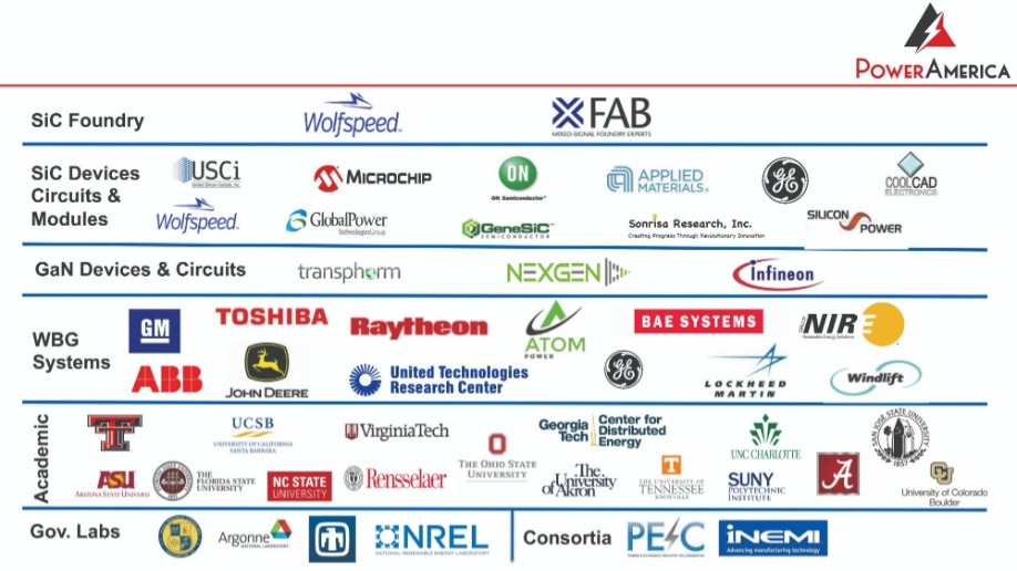
PowerAmerica is a 49 Strong, member driven institute active in all areas of the power wide bandgap supply chain


