

Better etching enhances selective area doping for vertical GaN power devices
Multi-step etching slashes the leakage current in regrown GaN p-n junctions for selective area doping.
BY HOUQIANG FU, KAI FU AND YUJI ZHAO FROM ARIZONA STATE UNIVERSITY
GaN is a very attractive material for making power electronics. It has a bandgap that is three times wider than the incumbent, silicon, and a critical electric field that is more than ten times higher. Thanks to these attributes, devices made from GaN can realise higher breakdown voltages when they have the same thickness as those made from silicon, or a similar breakdown voltage with less material. Additional strengths of GaN devices are a low on-resistance and a high switching speed, merits that are reflected in outstanding values for various figures-of-merit (see table 1).
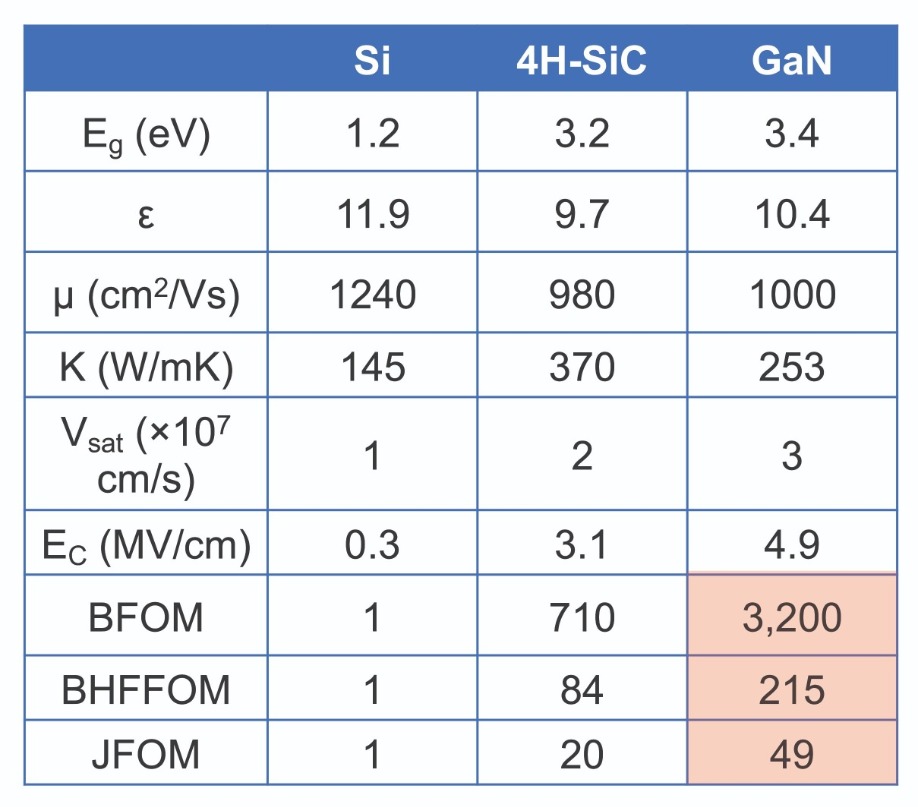
Table 1. Material properties and power electronics figures-of-merit (FOMs) for silicon, SiC and GaN. Eg: bandgap; ε: permittivity; µ: mobility; K: thermal conductivity; Vsat: saturation velocity; EC: critical electric field; BFOM: Baliga’s FOM; BHFFOM: Baliga’s high frequency FOM; JFOM: Johnson’s FOM. The FOMs of silicon are normalised to 1 to ease comparison.
However, these excellent material properties are of no practical benefit unless they are harnessed in electronic devices that excel on many fronts, and lead to efficiency gains in the likes of the power grid, electric vehicles, renewables, data centres, wireless charging, and consumer electronics.Building great GaN devices is far from trivial, with success hinging on the use of the best geometry.
Early development focused on lateral GaN power devices, such as HEMTs, grown on foreign substrates. With this architecture, breakdown voltages are held laterally, and currents flow laterally. That’s not ideal. Part of the problem is that there are issues associated with surface states that can lead to performance degradation, and also result in reproducibility and reliability concerns. In addition, the heat that is generated concentrates in a very narrow region, causing device temperature to rise; and the higher breakdown voltages require a larger chip area, an impediment to scalability.
To tackle these issues, our research team at Arizona State University has been developing high-performance vertical GaN power devices on bulk GaN substrates. One merit of this architecture is that it employs homoepitaxial growth, significantly reducing the density of defects, which can deteriorate breakdown voltages and increase leakage currents.
What’s more, the vertical device geometry offers: higher voltages and forward currents, without sacrificing chip area; better scalability and heat dissipation; and freedom from the effects of surface states.
This approach may raise a few eyebrows, given the high cost of GaN substrates. However, volumes have been steadily growing over the years, large size substrates with diameters of up to 6 inch are starting to emerge, and the substrate price is expected to continue to decrease, due to further expansion of both the power electronic market and that for GaN optoelectronic devices, such as laser diodes.
Vertical GaN power devices can be divided into four regions: the buffer layer, the drift layer, the channel layer and the edge-termination region (see Figure 1). We have strategies for improving each of these, leading to a boost in device performance. For the channel layer we are pursuing selective-area doping, an ongoing hot topic.
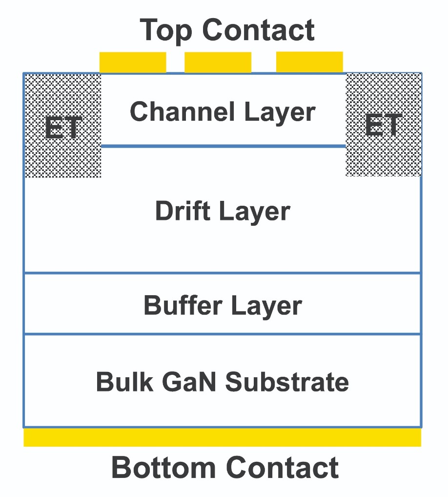
Figure 1. A cross-sectional diagram of the simplified structure of vertical GaN power devices on heavily doped bulk GaN substrates. ET indicates edge terminations
Doping challengesSelective-area doping remains a huge hurdle for realising the full potential of GaN power electronics. The purpose of this form of doping is to create laterally patterned p-n junctions (see Figure 2(a)). This type of junction is needed for the fabrication of various GaN power devices, including: junction barrier Schottky diodes or merged p-n/Schottky diodes (see Figure 2(b)); and vertical junction FETs (see Figure 2(c)). These structures have been produced in silicon and SiC by ion-implantation, but not in GaN.
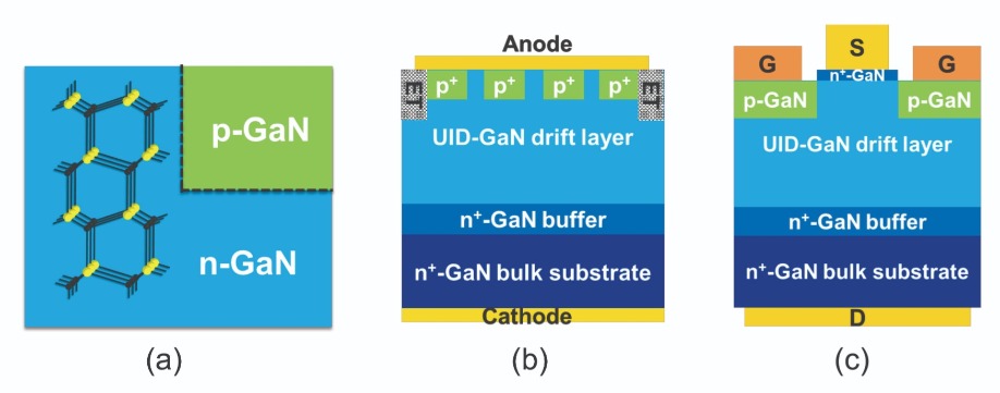
Figure 2. a) schematics of selectively doped p-n junctions. (b) JBS diodes or MPS diodes. (c) VJFETs.
There are two reasons why it is very challenging to realise ion-implantation in GaN, especially for the production of p-type material. One issue is related to the subsequent thermal annealing process, needed to activate implanted atoms and recover crystal damage caused by ion-bombardment. To anneal, often the temperature has to exceed 1200 °C, but GaN begins to decompose at only 900 °C.The second concern relates to the success of approaches to overcome this decomposition. To alleviate GaN decomposition at high temperatures, researchers have turned to capping layers such as AlN, multi-cycle rapid thermal annealing, and ultra-high pressure, but in all cases the conductivity of the implanted p-GaN is still very low – and judged from the perspective of power devices, it is far from satisfactory.
To overcome this particular hurdle, we have developed a re-growth method that realises selectively doped p-n junctions. With our approach, we can produce high conductivity p-GaN without having to worry about high annealing temperatures and associated GaN decomposition. This process currently remains one of the most important and promising methods for selective-area doping.
When we undertake our regrowth process, it is essential to ensure that the subsequent devices are not impaired by large reverse leakage currents, which can limit the ultimate breakdown voltage and increase power conversion losses in power electronics. Our research has uncovered two contributors to large leakage currents: surface contaminations at the regrowth interface, caused by impurities such as silicon, oxygen and carbon, all identified by secondary ion mass spectrometry; and etching damage, often caused by inductively coupled plasma etching, which is a widely used dry etching technique during GaN device fabrication.
To obtain selectively doped p-n junctions (as shown in Figure 2(a)), we could selectively remove part of n-GaN by inductively coupled plasma etching. This step would form trenches for subsequent p-GaN regrowth. However, this process would complicate experiments and analysis, because when two interfaces are exposed there is the possibility that leakage currents will flow in two directions. What’s more, this approach is time-consuming.
To avoid these complications and speed turnaround, we begin by making planar regrown p-n junctions (see Figure 3). These junctions, regrown by MOCVD, have provided us with a test vehicle for obtaining fundamental knowledge on regrowth, such as the impact of inductively coupled plasma etching and surface treatments.
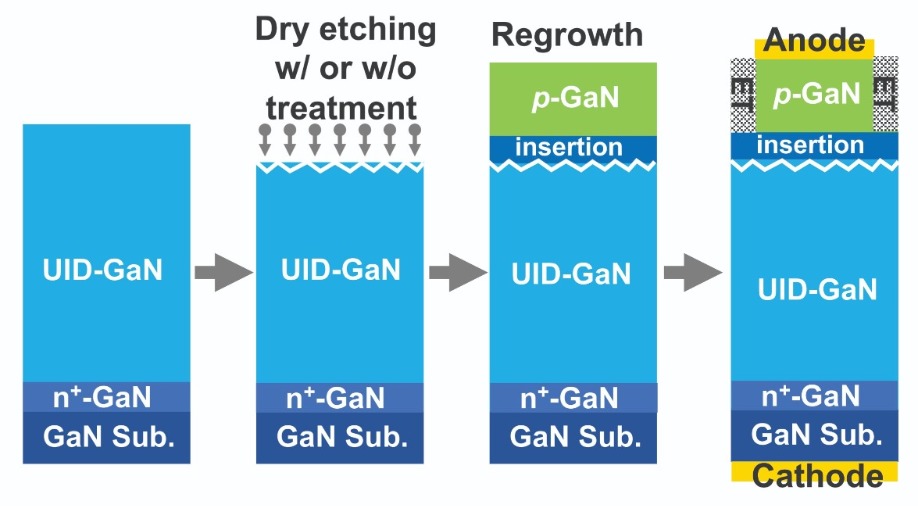
Figure 3. The growth and fabrication process of regrown p-n junctions formed by MOCVD. The structure is homoepitaxially grown on (0001) bulk GaN substrates. It is formed by the growth of an n+-GaN buffer layer and an unintentionally doped (UID) GaN drift layer, before undertaking ICP dry etching and surface treatments, followed by the regrowth of a thin insertion layer and p-GaN. Diode fabrication includes the deposition of metal stacks for anodes and cathodes, mesa isolation and edge termination.
Evaluating etching damageFor our first set of experiments, we co-load two samples into the MOCVD reactor and regrow without any surface treatment. With this approach, we compared a non-etched sample and one etched with an inductively coupled plasma etching power of 70 W. Both samples suffer from large reverse leakage currents, highlighting the need to properly treat the surface prior to regrowth.
To realise this, we adopt a combination of UV-ozone and acid surface treatments. The former utilises powerful oxygen radicals to oxidize the surfaces and organic residue contaminants. The beauty of this treatment is that it is purely chemical, and thus free from plasma discharging. Note that with inductively coupled plasma etching, ion-bombardment takes place that can lead to charging damage and deterioration of the device’s electrical characteristics. After the UV-ozone treatment, both samples are immersed in hydrofluoric acid and hydrochloric acid to remove oxidised materials and future clean the surface.
Electrical measurements reveal a massive reduction in the reverse leakage current in the non-etched sample. But that’s not the case in the etched sample (see Figure 4). Our hypothesis for explaining this stark difference is that in the etched sample, etching damage is so severe that it cannot be repaired by surface treatments.
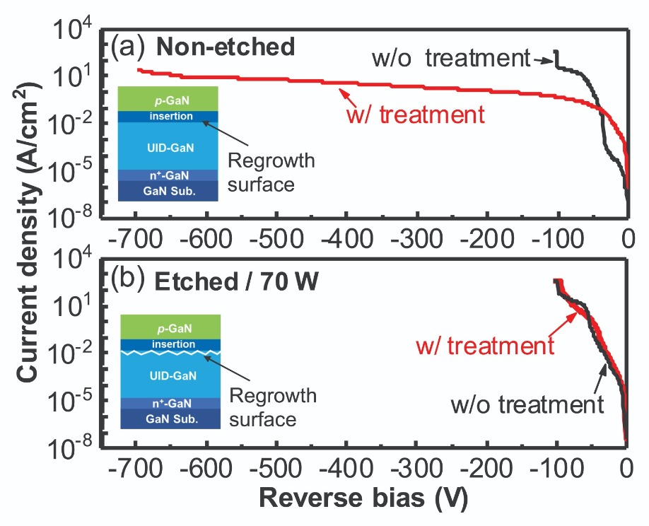
Figure 4. Reverse current-voltage characteristics of (a) non-etched and (b) etched samples with and without surface treatments. The non-etched sample was not subject to ICP plasma etching before regrowth. The etched sample was subject to ICP plasma etching, using a power of 70 W. Etching proceeds at around 200-300 nm/min, a reasonable rate for most device fabrication processes. A high etching power results in stronger ion-bombardment and more severe etching damage.
To put this theory to the test, we have carried out another set of experiments involving a lower etching power. This is reduced to just 5 W, a condition that slows the etching rate. We compare the reverse leakage currents in an as-grown sample with three samples that are first subjected to the aforementioned surface treatments. Two samples are etched with a power of 5 W, with an insertion layer thickness of 25 nm and 50 nm, respectively, and a third is etched at 70 W.Results indicate that slow etching dramatically reduces the reverse leakage currents, and that an insertion layer helps to move the junction away from the regrowth interface, further reducing the reverse leakage current (see Figure 5). For the etched sample with an inductively coupled plasma etching power of 5 W and a 50 nm insertion layer, the reverse leakage current is lower than that in the non-etched sample and similar to the as-grown sample. The key conclusion from this experiment is that the combination of slow etching and proper surface treatments is very effective for regrowth.
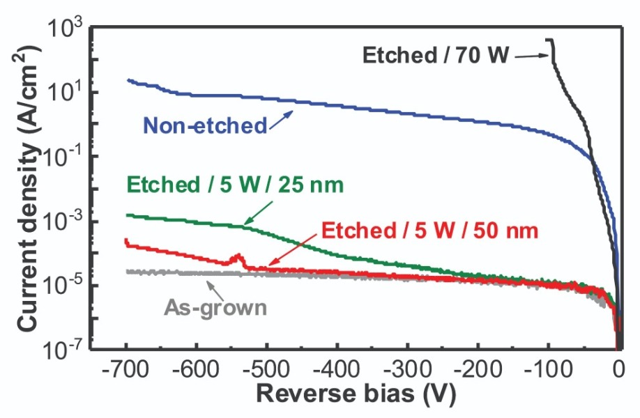
Figure 5. Reverse current-voltage characteristics of the non-etched sample and different etched samples. The power indicates the ICP etching power, and the thickness indicates the insertion layer thickness. An etching power of 5 W corresponds to an etching rate of around 20 nm/min.
Our findings prompt this question: What really drives the difference in reverse leakage currents between these samples? To find out, we have taken a closer look at the regrowth interface.One of its characteristics that can have a significant impact on the regrowth interface, and ultimately reverse leakage currents, is the charge density. Our measurements show that the higher the interface surface density, the larger the leakage current (see Figure 6). The as-grown sample has a low, constant charge distribution, on the order of 1016 cm−3, while the regrown sample has a peak charge density at the regrowth interface in the range 1017-1021 cm−3. Measurements also show that a reduction in the etching power lowers the charge density at the regrowth interface, and trims the leakage current.
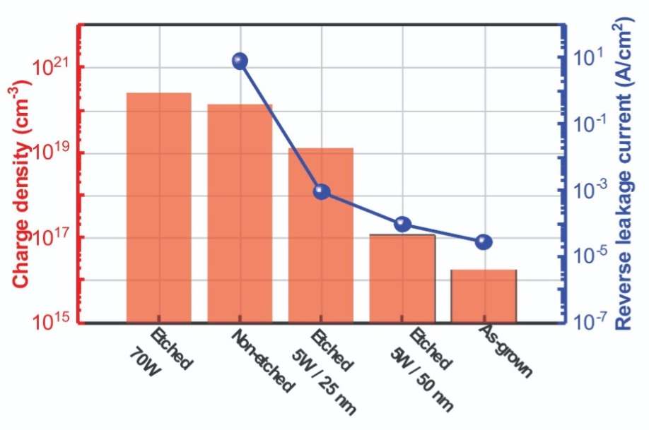
Figure 6. Charge density at the regrowth interface (histogram) and leakage current (line-shape) at −600 V for the five samples measured in Figure 5. The charge density is extracted from capacitance-voltage measurements.
It is not surprising that a high density of surface charges has profound physical consequences. These charges will create a large electric field at the regrowth interface, and help carriers to tunnel through the potential barrier in the p-n junction and make a significant contribution to the leakage current.Multi-step etching
Although slow etching delivers the best results, it’s not always practical. It can be very time-consuming, a significant impediment for some device structures with deep trenches and mesas.
To address this concern, we have evaluated multi-step etching, decreasing the ICP power from 70 W to 35 W, and then down to 5 W and finally 2 W. The four-step etching process pays dividends, producing samples with significantly reduced reverse leakage currents and the highest breakdown voltage – it can be over 1.2 kV (see Figure 7(a)).
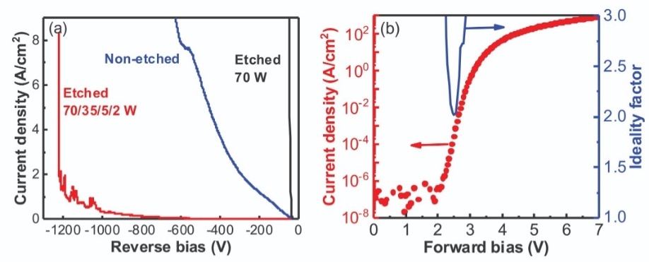
Figure 7. (a) Reverse current-voltage characteristics of the non-etched sample, the sample with the single-step etching, and the sample with the multi-step etching. All samples are subject to the aforementioned surface treatments. (b) Forward current-voltage characteristics and ideality of the sample with the multi-step etching.
Another benefit of this multi-step etching process is that it produces a good regrowth surface. We have compared two etched samples, both subject to a 70 W etching power. Subsequent slow etching steps, using multi-step etching, produce significant improvements in surface quality. We postulate that during multi-step etching, slow etching probably plays a role in recovering the plasma etching damage caused by previous high-power etching steps. In other words, slow etching is more like healing than etching.Before we can herald multi-step etching as a great success, we need to make sure that it doesn’t degrade the forward characteristics of regrown p-n junctions. Our measurements are encouraging. Samples exhibits excellent forward rectifying behaviours, with an on-off ratio of around 1010 and an on-resistance of 0.8 mΩ cm2. The ideality factor, which can be used to evaluate the performance of a p-n junction, is also promising. Its value is around 2.0, a figure that compares favourably with previously reported values for regrown p-n junctions, and is close to that of our as-grown samples – they are in the range 1.5-1.8.
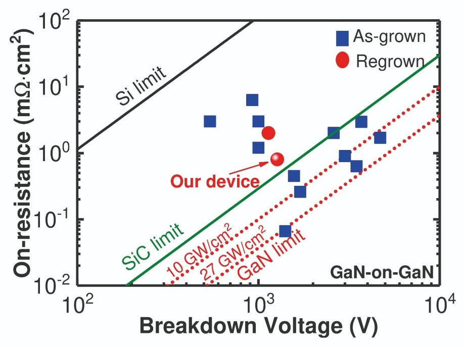
Figure 8. Benchmark plot of on-resistance versus breakdown voltage for reported as-grown and regrown GaN-on-GaN p-n diodes.
Baliga’s figure-of-merit provides another opportunity for us to benchmark our regrown p-n diodes. For these devices, it is 2.0 GW cm-2. That’s very close to the SiC limit, and even comparable to some values reported for as-grown p-n diodes. Given that this work is still in its infancy, we are very encouraged by this result. We anticipate improvements in inductively coupled plasma etching, surface treatments and device fabrications, spurring the performance of GaN regrown p-n junctions towards the GaN limit.In short, our results show that it is possible to produce high performance regrown p-n junctions via epitaxial regrowth. Our next step is to apply the obtained fundamental knowledge on regrowth to selective area doping. When progress follows, it will make a significant contribution to improving the performance of advanced GaN power electronics, and helping this class of device to create a greener planet.
K. Fu et al. Appl. Phys. Lett. 113 233502 (2018)
K. Fu et al. IEEE Electron Device Lett. 40 1728 (2019)
H. Fu et al. Appl. Phys. Express 11 111003 (2018)
H. Fu et al. IEEE Electron Device Lett. 39 1018 (2018)
H. Liu et al. Appl. Phys. Lett. 114 082102 (2019)


