
Moving photonics from lab to chip
Wide bandgap platforms will reduce the size and cost of applications within the UV to IR spectrum
A new paper in APL Photonics provides a perspective of the field of ultra-wideband photonic waveguide platforms based on wide bandgap semiconductors. These waveguides and integrated circuits can realise power-efficient, compact solutions, and move key portions of ultra-high-performance systems to the chip scale instead of large tabletop instruments in a lab, says author Daniel J. Blumenthal of University of California at Santa Barbara.
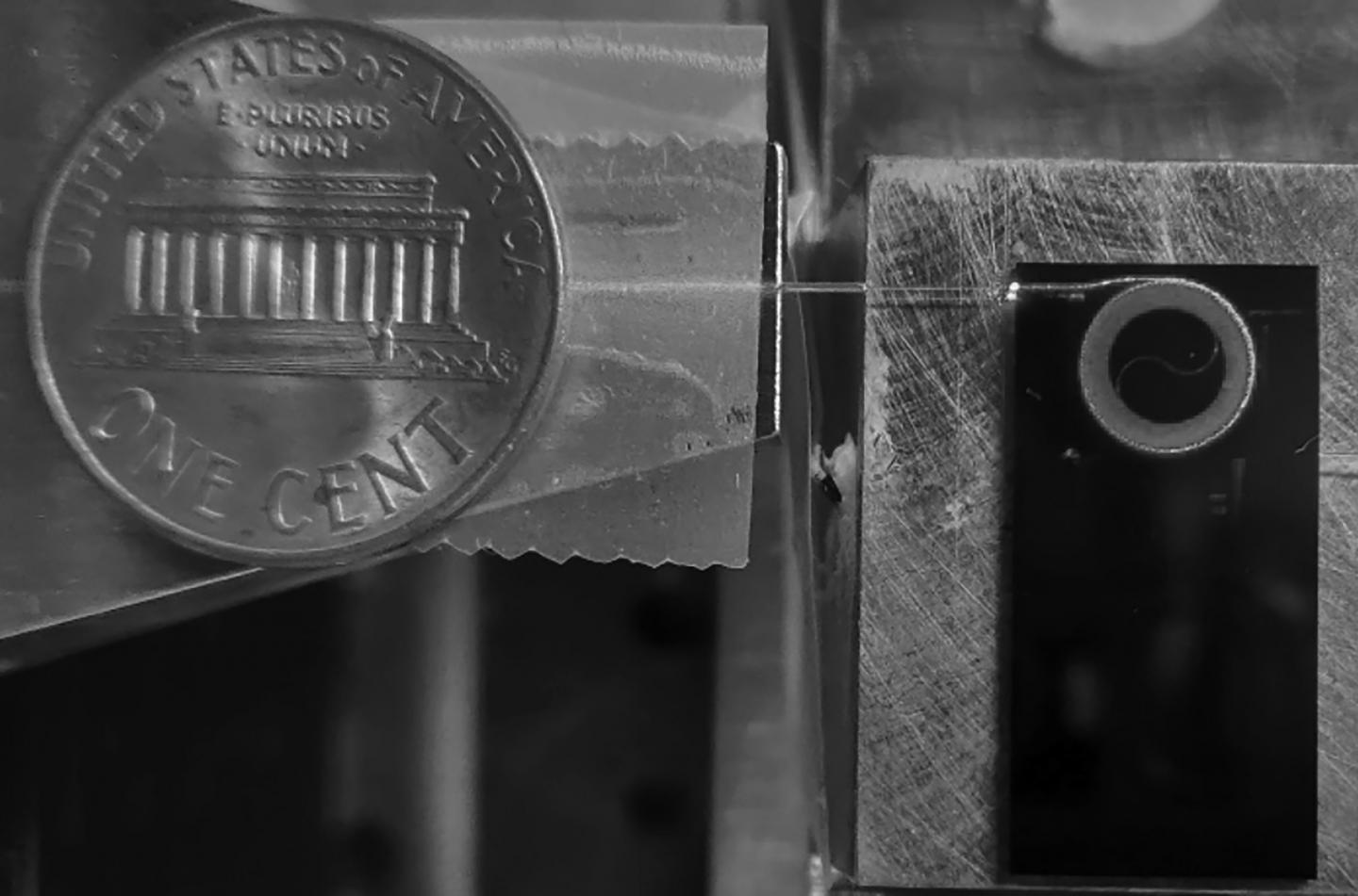
Blumenthal and his team have researched photonic integration platforms based on waveguides fabricated with wide bandgap semiconductors that have ultralow propagation losses.
"Now that the silicon market has been addressed for telecommunications and LIDAR applications, we are exploring new materials that support an exciting variety of new applications at wavelengths not accessible to silicon waveguides," said Blumenthal. "We found the most promising waveguide platforms to be silicon nitride, tantala (tantalum pentoxide), aluminum nitride and alumina (aluminum oxide)."
Each platform has the potential to address different applications such as silicon nitride for visible to near-IR atomic transitions, tantalum pentoxide for raman spectroscopy or aluminum oxide for UV interactions with atoms for quantum computing.
Applications, such as atomic clocks in satellites and next-generation high-capacity data centre interconnects, can also benefit from putting functions such as ultralow linewidth lasers onto lightweight, low-power chips. This is an area of increased focus as exploding data centre capacity pushes traditional fibre interconnects to their power and space limitations.
Blumenthal said next-generation photonic integration will require ultra-wideband photonic circuit platforms that scale from the UV to the IR and also offer a rich set of linear and nonlinear circuit functions as well as ultralow loss and high-power handling capabilities.
'Photonic integration for UV to IR applications' by Daniel J. Blumenthal; APL Photonics on Feb. 11, 2020


