
Semiconductor PbS can change its character
Swansea/Rostock team shows how rearrangement of atoms can make PbS behave like a metal or even a superconductor
The crystal structure at the surface of semiconductor materials can make them behave like metals and even like superconductors, a joint Swansea/Rostock research team has shown. The discovery, published in Advanced Functional Materials, potentially opens the door to advances like more energy-efficient electronic devices.
The research team, led by Christian Klinke of Swansea University's chemistry department and the University of Rostock in Germany, analysed the crystals at the surface of PbS nanowires.
By applying a method called colloidal synthesis to the nanowires, the team showed that the lead and sulphur atoms could be arranged in different ways and that this affected the material's properties.
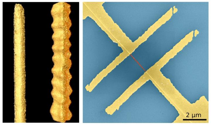
The picture above shows: Left - Shape of nanostructures made of PbS computer reconstructed based on series of transmission electron microscopy images. The left straight stripe behaves like a semiconductor and the right zigzag nanowire behaves like a metal. Right - Electrical device consisting of two gold electrodes contacting a nanowire (in red) on a silicon chip (in blue).
In most configurations the two types of atoms are mixed and the whole structure shows semiconducting behaviour as expected. However, the team found that one particular cut through the crystal, with the so called {111} facets on the surface, which contains only lead atoms, shows metallic character.
This means that the nanowires carry much higher currents, their transistor behaviour is suppressed, they do not respond to illumination, as semiconductors would, and they show inverse temperature dependency, typical for metals.
Mehdi Ramin, one of the researchers from the Swansea/Rostock team, said:"After we discovered that we can synthesise lead sulphide nanowires with different facets, which makes them look like straight or zigzag wires, we thought that this must have interesting consequences for their electronic properties.
But these two behaviours were quite a surprise to us. Thus, we started to investigate the consequences of the shape in more detail."
The team then made a second discovery: at low temperatures the skin of the nanostructures even behaves like a superconductor. This means that the electrons are transported through the structures with significantly lower resistance.
Christian Klinke of Swansea University and Rostock University, who led the research, said: "This behaviour is astonishing and certainly needs to be further studied in much more detail. But it already gives new exciting insights into how the same material can possess different fundamental physical properties depending on its structure and what might be possible in the future.
"One potential application is lossless energy transport, which means that no energy is wasted.Through further optimisation and transfer of the principle to other materials, significant advances can be made, which might lead to new efficient electronic devices.
"The results presented in the article are merely a first step in what will surely be a long and fruitful journey towards new thrilling chemistry and physics of materials."
'Function Follows Form: From Semiconducting to Metallic Towards Superconducting PbS Nanowires by Faceting the Crystal' by Mohammad Mehdi Ramin Moayed et al; Advanced Functional Materials; 16th March 2020


