

Comb lasers advance high-performance computers
By tackling a bottleneck in bandwidth, multi-wavelength quantum dot lasers are enabling improvements in high-performance computers
BY GEZA KURCZVEIL, DI LIANG AND Ray Beausoleil FROM HEWLETT PACKARD ENTERPRISE
Growth in data is occurring at a phenomenal rate. Now it takes just two years to produce 90 percent of all the data on the internet. That has major implications, particularly as it comes at a time when the performance of single cores has stagnated (see Figure 1 (a)).
To make headway, efforts are no longer directed at trying to increase the clock speed of single cores,
but are focused on the construction of processors with more and more interconnected cores, and
limited private memory on one socket. This new architecture makes much sense, given that memory is cheap, the opposite of what it was when the first computers were being built. In future, high-performance computers will feature a massive pool of memory at the centre, surrounded by many compute nodes located at the periphery, with all nodes having access to the full memory pool (see Figure 1 (b)).
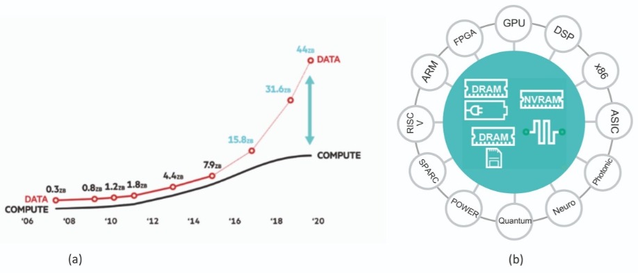
Figure 1. (a) While memory has gotten cheaper over time and there has been an exponential rise in the generation of data, single-thread performance has stagnated. (b) In memory-driven computing a massive pool of memory is at the centre of the architecture, and application-specific compute nodes are placed at the periphery. Each compute node has access to the full memory pool.
A key requirement for this new high-performance computer architecture is a massive communication link for the massive pool of memory. Without this, there would be insufficient throughput of data between memory and compute nodes.One option for the data link is electronic interconnects, such as copper wires. However, they suffer from significant losses, high power consumption, and cross-talk at higher frequencies. A far better alternative is optical interconnects, which address all the weaknesses of wires while allowing the transmission of multiple wavelengths. Data can be transmitted through these links using a technology known as wavelength division multiplexing, which avoids any crosstalk between channels. It is a well-established approach for routing internet traffic when distances and bandwidths are large enough to justify the cost – and as deployment has increased, prices have fallen, making these links common-place in applications where distances are on the order of just a metre. As that’s a length scale found in high-performance computing, optical links are already used for rack-to-rack connections.
High-performance computers require aggregated data rates of terabits per second. Today, this rate is out of the reach of a single laser, so the aggregated data rate is sliced up between many lasers, each making an equal contribution. Although individual lasers can transmit at above 200 Gbit/s, data rates of only up to 20 Gbit/s are actually used, to minimise energy consumption.
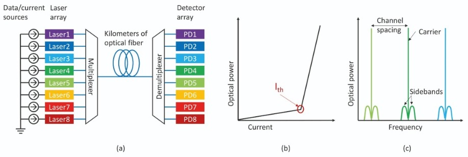
Figure 2. (a) A typical optical link consisting of several single-wavelength lasers. Data are encoded on the optical signal by turning each laser on and off. (b) The output power of a laser as a function of injection current. Once data are encoded onto a laser signal, sidebands are generated. As long as the sidebands of neighbouring channels do not overlap, there is no crosstalk between channels. This is accomplished by limiting the modulation speed.
A common approach for operating these lasers is amplitude modulation. But this has a downside, producing sidebands above and below the original optical carrier wavelength (see Figure 1 (c)). Due to this, the sidebands of one channel have to be sufficiently separated from those of the neighbouring channels to minimise crosstalk. When driving a laser with amplitude modulation at a data rate of 50 Gbit/s, there needs to be a 3.5 THz channel spacing to minimise crosstalk.To transmit data using wavelength-division multiplexing, signals from a number of lasers are united by an optical multiplexer, routed through a fibre, and sent to a demultiplexer that returns the data back to a collection of signals at different wavelengths. Photodetectors then convert all of these signals into electrical signals, which is the form required by today’s processors and memory. Note that this scheme, which works very well, is particularly attractive for links with low-to-medium volumes of traffic, because it allows unused channels to be turned off, saving power.
Unfortunately, wavelength-division multiplexing is not easy. There are often imperfections in the laser production process, resulting in variations in the lasing wavelength. Addressing this requires active monitoring and tuning. If there are many channels, and the spacing is below 100 GHz – this is the case in dense wavelength division multiplexing – variations in wavelength can create significant problems. In such situations, rather than using many single-wavelength lasers, it is better to use one laser that provide multiple wavelengths – a comb laser.
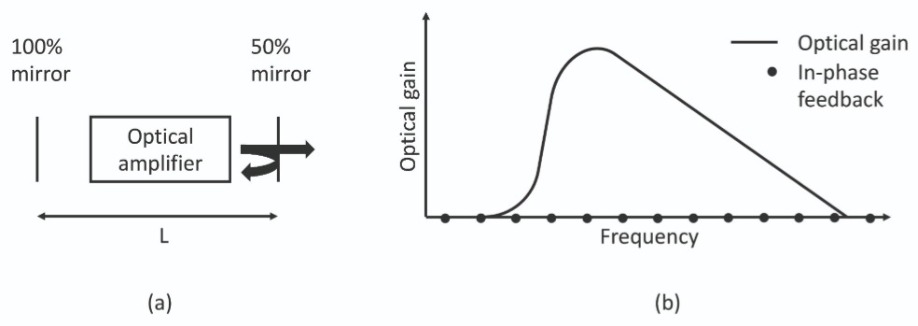
Figure 3. (a) A basic laser cavity contains an optical gain amplifier, surrounded by a pair of mirrors. (b) Lasing occurs at frequencies where light experiences a positive net gain and the feedback from the mirrors is in phase with the light in the cavity.
Comb credentialsA key difference between a conventional, single-wavelength laser and that with a multiple wavelength comb is the reflectivity of the mirrors. Conventional lasers need an additional bandpass filter inside the cavity – or at least a narrow-band mirror – to ensure single-wavelength lasing, while comb lasers employ a more straightforward design, tending to consist of a long cavity and broadband mirrors (see Figure 3(a)). For cleaved lasers, which can be formed with cleaved facets, the cavity can be 0.5 mm or longer, depending on the desired channel spacing.
With a comb laser, the spacing between the lines is fixed. Although changes in temperature shift the entire comb to either higher or lower wavelengths, once one knows the wavelength of one of the comb lines, one knows the wavelengths of them all. That’s because the channel spacing is determined lithographically, and it is therefore a prescribed, controllable design parameter.
Given the great simplicity of the design of the comb laser, one may wonder why anyone would ever go to the trouble of making a single-wavelength laser. The reason is that when a comb laser is built with the most commonly used optical gain medium – a stack of quantum wells – this device is impaired by an intrinsic material property known as mode partition noise. This impediment produces random fluctuations in optical power for every comb line. Although these fluctuations, occurring on a nano-second timescale, do not alter the total optical power, they are a show-stopper for error-free data transmission. That’s because it is not possible to transmit an optical ‘one’ while the power of a comb line has randomly dropped to zero.
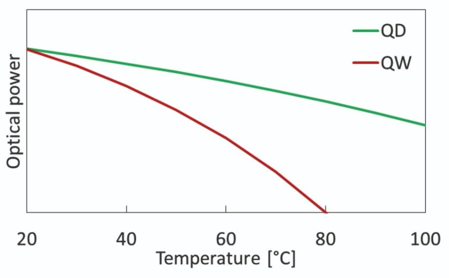
Figure 4. As the temperature of the laser junction increases, optical output power decreases. Due to the three-dimensional confinement of electrical carriers, the power drop in quantum-dot lasers is far smaller than in traditional quantum-well lasers. This makes quantum-dot lasers especially attractive for applications where temperature control is impossible or limited.
So why have comb lasers suddenly risen in popularity, given these issues? Ironically, the recent success has nothing to do with comb lasers. Instead, progress has been driven by the development of a relatively new gain medium, quantum dots. Researchers in Japan pioneered these low-dimensional structures, developing a laser with greater tolerance to temperature variations. By switching from wells to dots they were able to increase the confinement of electrical carriers, with early experimental work verifying an increase in high-temperature gain stability (see Figure 4). After this success, it took a few more years until a collaboration between researchers in Germany and Russia investigated the topic of mode partition noise in quantum dot comb lasers. This work revealed that the introduction of dots quashed the partition noise in these devices.Not all comb lasers are created equally. Some are more practical than others for data communication, because they combine a low mode partition noise with a flat comb that ensures that all channels have similar signal-to-noise ratios. Poor candidates for high-performance computing include lasers with frequency combs generated in SiN resonators, as they show a Gaussian distribution of comb line amplitudes (see Figure 5 (a)). The good news, for reason yet to be understood, is that the combs from quantum-dot lasers produce flat spectra with a relatively uniform power over a large number of comb lines (see Figure 5 (b)). However, not all comb lasers are suitable, as there are problems with pulsed variants (for details see the box “The problems of pulsed comb lasers”).
Encoding independent data streams on each comb line is not as straightforward as for a single-wavelength laser. Turning the laser on and off by modulating its injection current encodes the same data stream on all the comb lines, which is inefficient.
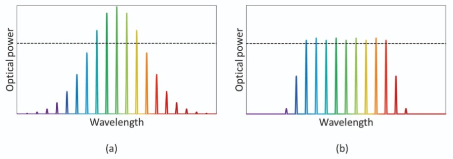
Figure 5. (a) Some comb lasers exhibit a Gaussian distribution of amplitudes. The dashed line indicates a hypothetical power level for noise-free data transmission. Comb lines with less power cannot be used, so they reduce the device efficiency. (b) Quantum-dot-based comb lasers produce a more rectangular optical spectrum. This device has the same total power as the one in (a). Note that more channels satisfy the power requirement for noise-free data transmission.
Instead, our team at Hewlett Packard Enterprise has the comb laser on at all times (see Figure 6) and places several micro-ring modulators outside of the laser – we have one for each comb line (see Figure 7 (a)). This approach exploits a key characteristics of micro-ring modulators, a wavelength dependent loss (see Figure 7 (b)). By adjusting the voltage of the p-n junction of the micro-ring, we shift the wavelength of maximum loss, which is the resonance wavelength. To generate an optical ‘one’, we tune the resonance wavelength away from the comb line; and to produce a ‘zero’, we line-up the resonance wavelength with the comb line.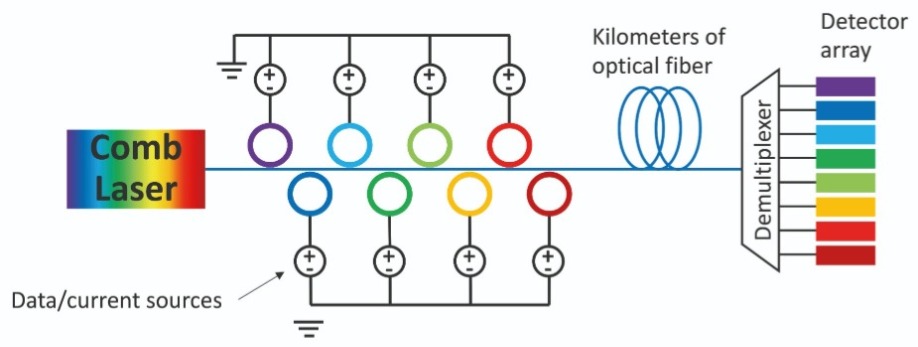
Figure 6. An optical link based on a comb laser. Rather than directly modulating the laser, external modulators are used to encode data on individual comb lines.
Our micro-ring modulators are compact, with a diameter of around 10 µm. With proper design, they can transmit data at 50 Gbit/s. The full-width-half-maximum of the micro-ring’s resonance is ideal, being wide enough to capture an entire comb line, but narrow enough to allow neighbouring comb lines to be transmitted without any loss in optical power. Selecting the resonance wavelength of the micro-ring is relatively easy, as it can be tuned by adjusting the diameter of the ring, its inner width, and its thickness.One of the constraints of micro-ring modulators is that they impose a limit on optical power. If it is too high, non-linearities degrade the contrast of the resonance, and in turn lower the signal-to-noise ratio of the encoded data (see Figure 7 (b)). Due to this restriction, it is far better to operate comb lasers with a constant optical power. Fortunately, that’s a great operating regime for this class of laser, thanks to its gain recovery characteristics.
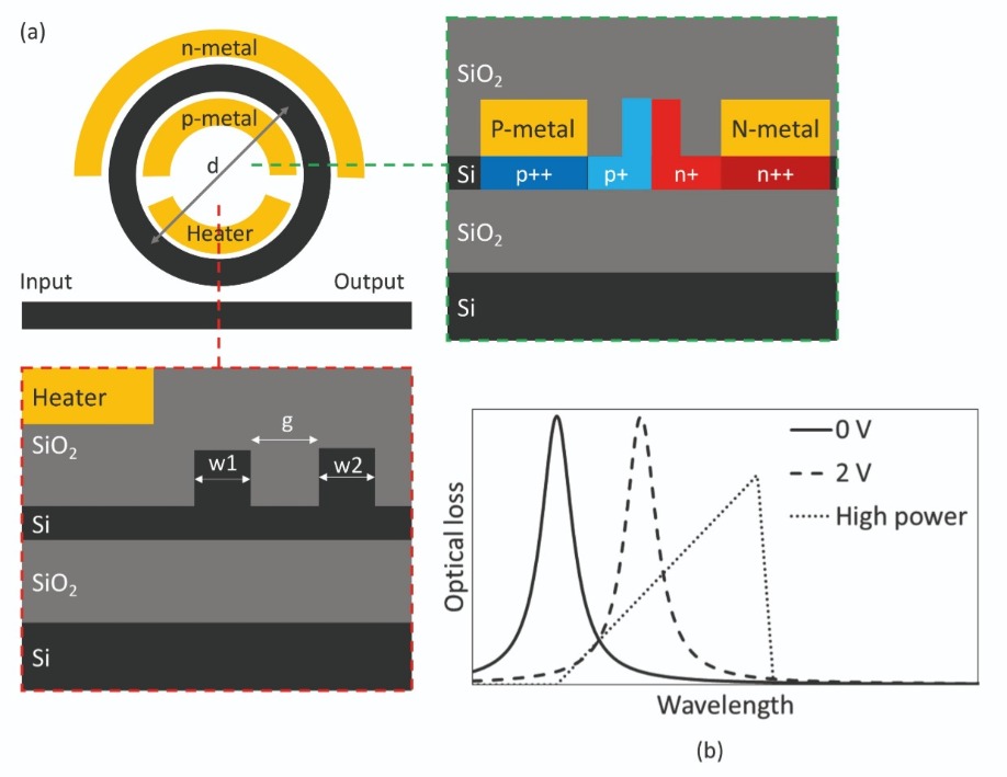
Figure 7. (a) Top-down and cross-sectional diagrams of a micro-ring modulator. (a) The wavelength-dependent loss of a ring modulator has a resonance that can be engineered using parameters d, g, w1, and w2 in (a). In addition, it can be tuned using a power-hungry heater. Data are encoded by applying a voltage across the p-n junction. (b) The shape of the modulator’s resonance becomes highly distorted at high optical powers, making pulsed lasers less desirable as a light source.
There will always be a shift in the lasing wavelength of the comb laser, even if the micro-ring is perfect. What’s needed is some form of tuning or tracking to maintain a line-up between the ring’s resonance wavelengths and the temperature-shifted comb lines. One option is to apply a voltage to the p-n junction, but this results in excess optical loss, in the form of free-carrier loss.The common way to avoid this is to use a resistive heater to locally change the ring’s temperature. In turn, this shifts the refractive index of the cavity, and can deliver large changes to the resonance wavelength. However, resistive heaters are wasteful, requiring up to tens of milliwatts to shift the wavelength by just a nanometre.
We prefer a more energy-efficient approach, using a capacitor to tune the resonance wavelength. With our design, a layer of semiconductor material is placed on top of the micro-ring, and inserted between is a 20 nm-thick layer of dielectric, such as SiO2 or Al2O3 (see Figure 8). Electrodes are added to the silicon and the semiconductor to form a metal-oxide-semiconductor capacitor. When a voltage is applied to this device, sufficient electrons and holes accumulate at the dielectric interfaces to produce a change in the refractive index of the micro-ring, and its resonance wavelength. As the current flowing through the capacitor is incredibly small – it is only around 100 fA – the resulting tuning is 10-9 mW/nm, giving an increase in efficiency of nine orders of magnitude compared with a resistive heater.
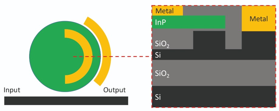
Figure 8. A MOS tuner provides much more efficient resonance tuning than a thermal tuner. When a voltage is applied to the contacts, charges accumulate at the SiO2 layer, which is between the silicon and the InP. Charge accumulation is sufficient to change the refractive index and thus the resonance wavelength. However, since no current flows through the capacitor, power consumption is negligible.
To manufacture these comb lasers in high volume, using a high yield, low-cost process, they must be integrated on silicon substrates. Our short-term solution is to take GaAs-based epitaxial wafers, which contain our quantum dot structures, and use a molecular bonding technique to attach them to silicon-on-insulator wafers. We then selectively remove the GaAs substrate to leave a 1-2 µm-thick epitaxial stack on silicon, and process this material in the same way that is used to produce conventional GaAs lasers. However, we have the benefit of using much larger, stronger wafers.A great strength of this process is that the silicon layer in these lasers provides both a mechanical substrate and an optical waveguide (see Figure 9 (a)). Silicon is ideal for waveguiding – it has a far lower optical loss than those made with GaAs or InP systems, and it allows us to make: high quality laser mirrors; MOS tuners for near zero-power tuning; and vertical grating couplers, which allow rapid, wafer-level device testing. With this approach we have fabricated comb lasers operating up to 100 °C (see Figure 9 (c)), and variants that provide 14 channels for error-free, high-speed modulation (see Figure 9 (d) and (e)).
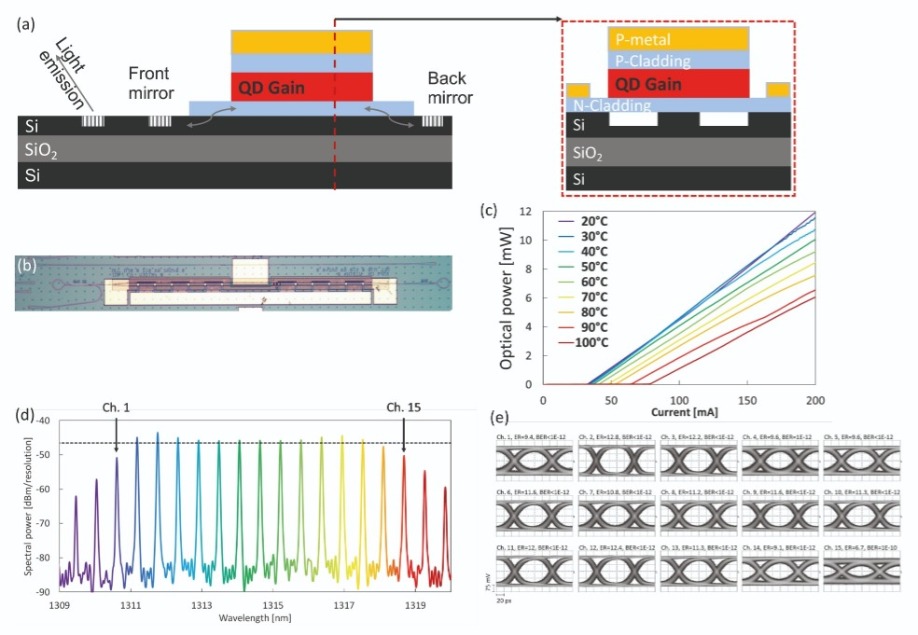
Figure 9. (a, b) Cross-sectional diagrams of a quantum-dot comb laser on a silicon-on-insulator substrate. Thin epitaxial layers between the top silicon and the quantum-dot gain allow efficient transfer of light between them. (b) Top-down photograph of a fabricated comb laser on silicon using wafer bonding. (c) Optical output power as a function of current and temperature showing excellent high-temperature performance. (d) Optical spectrum of a comb laser showing multiple comb lines with a quasi-rectangular shape. 12 comb lines within 3 dB of the peak (dashed line) are observed. (e) Eye-diagrams and bit-error-ratios (using an external modulator) showing error-free performance in 14 of the 15 channels that were measured (the bit error rate is no more than 10-12).
Longer term, our plan is to produce comb lasers by growing quantum-dot-containing layers directly on silicon. This is far from easy, due to the large lattice mismatch between silicon and GaAs. Left unchecked, this results in a high density of defects that drag down device reliability, and can even kill lasing operation in an instant. Some groups have turned to thick buffer layers to reduce the strain in the quantum dot layers, but this hampers efficient coupling of light from the quantum dot layers to the silicon. Due to this, teams that have made devices that are based on direct growth of quantum dots on silicon have only used silicon as a mechanical carrier.While comb lasers are very attractive, we are not advocating their use in every optical link. Since all channels in a comb laser are always on, comb lasers are only attractive for dense wavelength division multiplexing links that have a high volume of traffic at all times. Use a comb laser with many channels in a link with little traffic, and lots of power will be wasted by the unused channels, because they cannot be turned off. For links with low and medium levels of traffic, using an array of single-wavelength lasers may offer a more energy efficient solution.
There are two remaining challenges to overcome before comb lasers are ready to light up the next generation of high-performance computers. The first of these is device reliability. Since all channels are created in one laser, when a device fails, it impacts all channels. One way to partly offset this risk is redundancy.
The second challenge is to devise an effective approach to increasing the number of channels. Although the spacing between the channel is inversely proportional to the length of the laser, making a laser longer is not a recipe for success. What happens is that as the channel spacing gets narrower, the individual channel rate has to be reduced to maintain a low cross-talk between the channels. The upshot is that there is no increase in the aggregated bandwidth.
A more promising solution is to increase the width of the optical window for the comb lines. The upper limit for this is determined by the gain bandwidth of the optical amplifier, which is typically 50 nm wide. Through engineering, this has the potential to be increased to more than 100 nm. However, even for ‘regular’ optical amplifiers with a 50 nm gain bandwidth, the combs that result are typically just 15 nm wide. At present, the reason for this is unclear, but several hypotheses have been suggested.
One possible explanation is spatial hole burning, and another is group velocity dispersion – that there is imperfect mode spacing of a comb, resulting from a wavelength-dependent refractive index. If either of these are the cause, they can be addressed by engineering. Analytical models are being developed to help understand the impact of these phenomena, and experiments are underway to verify the models. When success follows, we shall be a step closer to implementing the efficient, high-speed optical links required to maintain progress in high-performance computing.
When comb lasers produce a pulsed output, or are temporally modelocked, the average optical output power is constant, but the energy of one period is compressed (see figure below). This can cause two problems. One potential issue is that the higher instantaneous power, contained in pulses typically as short as 2 ps, accelerates device failure, such as catastrophic optical mirror damage. This is particularly problematic in comb lasers, as a failure impacts all channels. The second issue is that the high output power of the peaks impairs the contrast of the resonance, and ultimately reduces the signal-to-noise ratio of the encoded data.
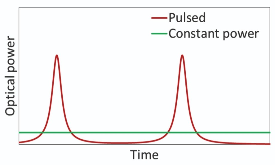
Pulsed lasers are a form of comb laser that emit periodic pulses. The two devices shown here have the same average power, but the pulsed laser has a much higher peak power than the constant-power laser. The presence of pulses can have unwanted consequences such as reduced laser reliability and reduced signal-to-noise ratio of the encoded optical data.
D. A. B. Miller Proc. IEEE 97 1166 (2009)
D. A. B. Miller J. Lightwave Technol. 35 346 (2017)
K. Bresniker et al. IEEE Computer, December 2015
R. G. Beausoleil et al. IEEE J. Sel. Top. Quantum Electon 19 3700109 (2013)
M. J. R. Heck et al. IEEE J. Sel. Top. Quantum Electron 19 6100117 (2013)
M. Sugawara et al. Nature Photonics 3 30–31 (2009)
A. Gubenko et al. Electronic Letters 43 1430 (2007)
W. Bogaerts et al. Laser and Photonics Reviews 6 47 (2012)
D. Liang et al. Nature Photonics 10 719 (2016)


