

Stacking GaN and silicon transistors on 300 mm silicon
Next-generation mobile devices, data infrastructure and communication networks could be aided by three-dimensional, monolithic integration of GaN and silicon CMOS on 300 mm wafers
BY HAN WUI THEN FROM INTEL CORPORATION
THE TRANSITION to 5G and beyond is tipped to drive an exponential increase in the number of connected mobile devices. The integrated circuits that power them will need to provide greater energy efficiency, in a smaller form factor. Consequetly, there is much demand for more capable transistors and the integration of ever-larger numbers of components on the microchip.
Fulfilling these requirements is far from easy, as none of today’s transistor technologies are capable of meeting the diverse needs associated with power delivery and RF front-end design. Due to this issue, circuit designers are combining many distinct, separate chips. This is not great, as it results in a bulky package.
To tackle this problem, our team at Intel’s Components Research division in the Technology Development Group of Oregon has developed the first monolithic, three-dimensional GaN and silicon transistor stacking technology. It delivers best-in-class performance and efficiency, while allowing diverse functionalities to be integrated on a single chip.
Combining silicon and GaN is an attractive proposition. Silicon is today’s workhorse for power electronics and RF switches, but it struggles to deliver high-frequency, high-power performance, so it is not a good choice for RF power amplification (see Figure 1). For that particular task, GaAs HBTs, GaAs HEMTs and GaN HEMTs are the front runners. However, these technologies are not ideal for making efficient power electronics: depletion mode GaAs HEMTs and GaN HEMTs are not favoured, due to their always-on nature; and the GaAs HBT is unsuitable, being current-driven rather than field-driven.
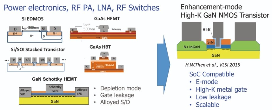
Figure 1. In today’s power delivery and RF front-end solutions, dissimilar technologies come in multiple distinct and separate chips that have to be made to work together in a bulky package. Enhancement mode GaN transistors enabled by high-κ dielectric and metal gate technology can enable, for the first time, all these functionalities to be integrated on a single chip, realising a system-on-chip (SoC).
Fortunately, there is a transistor that excels on all fronts: the enhancement-mode (e-mode) GaN transistor. Recently, we have shown that when this class of device is equipped with high-κ dielectric metal gate technology, it can deliver best-in-class performance, in both power delivery and RF front-end functionalities. We have built on this success by using three-dimensional monolithic integration to unite GaN power and RF transistor technology with silicon PMOS on 300 mm silicon substrates. Thanks to this, all functionalities can be integrated on a single chip to yield a system-on-chip for the very first time.One of the successes that has come from our efforts is the fabrication of the first high-performance GaN transistors on 300 mm silicon (111) wafers (see Figure 2). We make these transistors with a 300 mm process technology that is compatible with leading CMOS fabs.
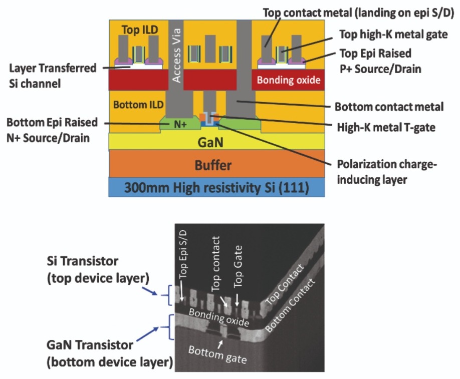
Figure 2. Intel has produced the first GaN transistors on a 300 mm silicon (111) wafer in one of its leading CMOS fabs. Its researchers have employed a new technique of three-dimensional monolithic integration by layer transfer to stack silicon PMOS transistors on top of GaN NMOS transistors to enable CMOS functionalities, for the first time in industry.
Another accomplishment is our use of a new technique of three-dimensional monolithic integration, based on layer transfer. With this approach we are breaking new ground by stacking silicon PMOS transistors on top of GaN NMOS transistors to enable CMOS functionalities. This new technology significantly expands the universe of solutions that can be implemented and integrated in an efficient, tiny system-on-chip.Using one of our leading CMOS fabs for processing our GaN transistors on 300 mm silicon reaps an additional reward – it opens the door to all the latest process innovations. They include high-κ technology, three-dimensional layer transfer, chemical-mechanical polishing, lithographic techniques and copper interconnects. In addition, we benefit from the significant reduction in cost associated with cheaper 300 mm silicon substrates and high-volume production.
Leveraging larger wafers
Due to the lack of native substrates, nearly all GaN is grown on foreign substrates, such as sapphire, SiC and silicon. The most popular platforms are 3-inch and 4-inch SiC, which are both relatively expensive, and 4-inch, 6-inch and 8-inch silicon (111). In contrast, we are using cost-effective 300 mm silicon (111) substrates (see Figure 3). On this platform we marry GaN with the most advanced high-κ dielectric metal gate technology in our 300 mm fab. This enables enhancement-mode operation and gate-stack scaling, and it ultimately realises high performance and low leakage, the keys to higher efficiencies. Note that this reduction in leakage is significant – it can exceed four orders of magnitude (see Figure 4) better than a Schottky gate GaN HEMT.
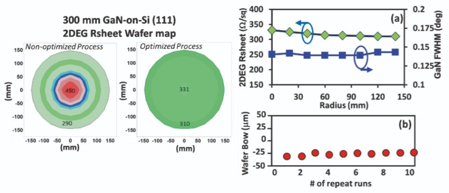
Figure 3. Optimised and uniform data from a manufacturable 300 mm GaN epitaxy process at Intel. Data distributions shown include: two-dimensional electron gas sheet resistance; GaN crystal quality, evaluated in terms of the the x-ray diffraction peak’s full width at half-maximum (FWHM); and 300 mm wafer bow.
Another virtue of enhancement-mode, GaN transistor technology is that it simplifies the circuit architecture. As the enhancement mode transistor is normally-off, it does not require a negative power supply. Instead, this device can be driven directly from a battery, saving precious real estate on the microchip.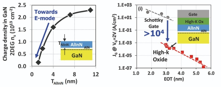
Figure 4. A high-κ gate dielectric reduces gate leakage by more than four orders of magnitude at scaled equivalent oxide thickness (EOT) for higher performance.
Measurements on our high-κ dielectric enhancement-mode GaN NMOS transistors on 300 mm silicon reveal excellent electrical characteristics and best-in-class performance for power delivery and RF. The devices have low drain leakages, high drive drain currents, low knee voltages and low on-resistances. Such characteristics show that high-κ dielectric technology enables a GaN transistor to combine a low leakage with excellent performance – it is about four times better than industry-standard silicon transistors for power delivery (see Figure 5).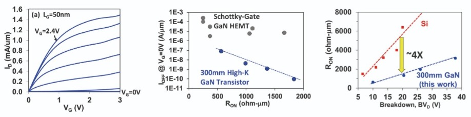
Figure 5. The ID-VD characteristics of Intel’s e-mode high-κ dielectric GaN NMOS transistor on a 300 mm silicon wafer showing a high drive drain current that is approaching 1.5 mA/mm, a low knee voltage (it is below 1 V), and an on-resistance, RON, of just 610 W-Ωm. Low drain leakage, with IOFF as low as 100 pA/mm at 5 V drain voltage, and excellent RON can be achieved simultaneously. The high-κ e-mode GaN NMOS transistors are about four times better than silicon transistors used for power delivery.
Our devices also deliver excellent RF performance. Our high-κ GaN NMOS transistor significantly outperforms those based on GaAs and silicon/SOI transistors in power-added efficiency across a wide frequency range that spans 1 GHz to 30 GHz (see Figure 6). Due to the excellent knee voltage and on-resistance, efficient power amplifier (PA) operation is realised at drain voltages as low as 1 V (see Figure 7).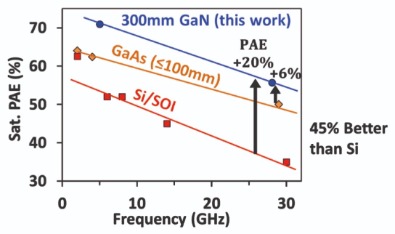
Figure 6. Intel’s high-κ e-mode GaN NMOS transistor significantly outperforms GaAs and silicon/SOI across a frequency range spanning 1 GHz to 30 GHz.
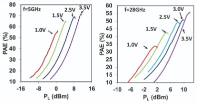
Figure 7. High power-added efficiencies are demonstrated with supply voltages from 3.5 V to as low as 1 V. Efficient PA operation well below 2 V surpasses the minimum cut-off supply voltage achievable by typical GaAs HBTs and highlights the potential of Intel’s high-κ GaN transistor to extend battery life, and to realise efficient envelope-tracking RF PA.
This value is well below the minimum cut-off supply voltage for a typical GaAs HBT, highlighting the potential of the high-κ GaN NMOS transistor to significantly extend battery life while providing unrivalled efficiencies using the envelope-tracking RF PA architecture. High-κ GaN NMOS transistors also make excellent RF switches and low-noise amplifiers. For example, they have an excellent figure-of-merit for the switch, with a product of on-resistance and off-capacitance of just 110 fs. The minimum noise figure is only 0.4 dB at 5 GHz and 1.36 dB at 28 GHz (see Figure 8).
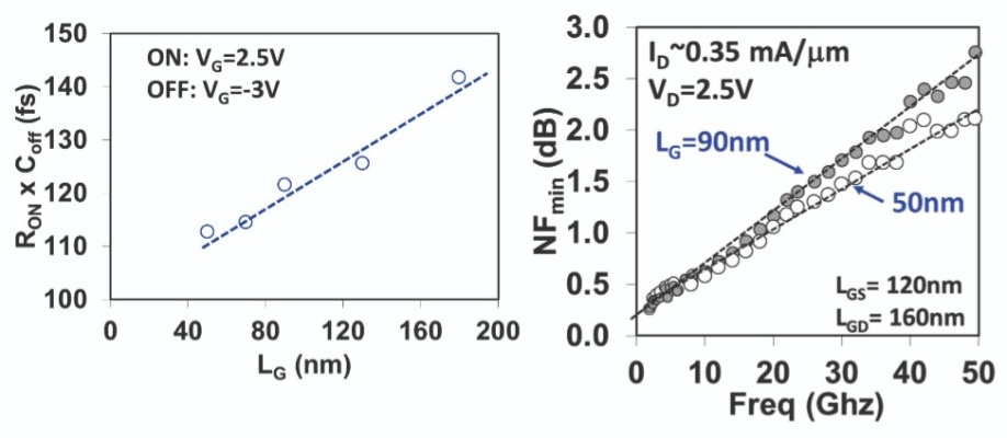
Figure 8. The excellent switch figure-of-merit, RON x COFF, and noise performance, NFmin, of the high-κ e-mode GaN NMOS.
The combination of the great performance as a power amplifier, a low-noise amplifier, an RF switch and a power transistor enables the enhancement-mode high-κ GaN NMOS transistor technology to boost the efficiency and performance of RF front-end and power delivery systems beyond what is capable today with GaAs and silicon technology. But that’s not all – by turning to high-κ GaN NMOS transistor technology, we realise compact integration of multiple functionalities on a single chip, saving space and achieving unmatched small form factors.Three-dimensional integration
A selling point in today’s marketplace is tight on-chip integration of CMOS analog and digital logic/control functionalities, along with CMOS memory. These types of CMOS chips are currently built as standalone units, but as functionality and complexity increases, monolithic system-on-chip solutions will be needed to provide higher efficiency, lower cost and a higher integration density (see Figure 9).
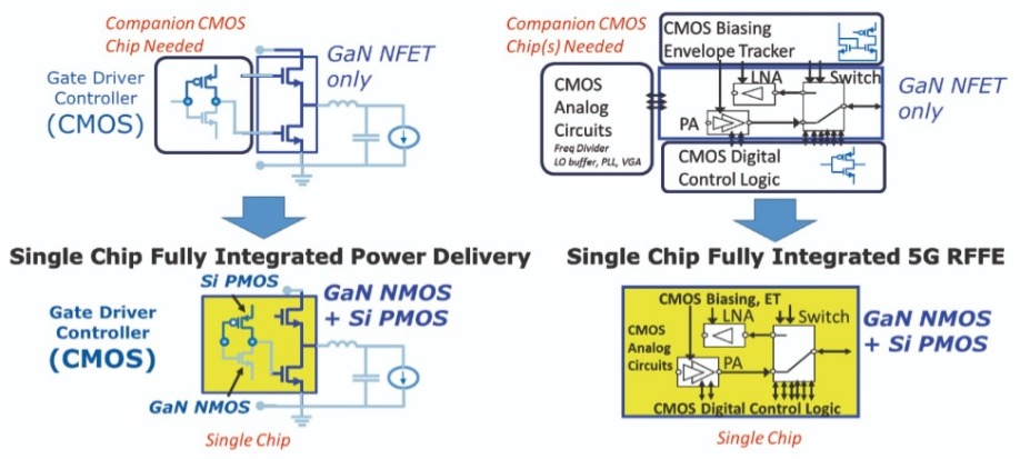
Figure 9. Single-chip fully integrated power delivery and RF front-end units can be realised with Intel’s three-dimensional monolithically integrated silicon PMOS stacked on GaN NMOS transistor technology.
However, it is extremely challenging to implement a design based on monolithic complementary GaN CMOS, due to the low hole mobility in GaN, and the difficulty in realising high p-type doping in this material. The good news is that progress is being made by a partnership between our team and research groups at Cornell and MIT. This effort hopes to fulfil the promise of wide bandgap, high-voltage operation of GaN PMOS. While this work is in its infancy, the hope is that standard high-κ metal gate silicon PMOS can step in to provide an excellent complementary p-channel technology to GaN NMOS, due to its high hole mobility and possibility to realise a very high p-doping for source-drain contacts.To monolithically integrate multiple dissimilar semiconductor materials on a single silicon substrate, we have turned to layer transfer techniques. This enables us to monolithically stack silicon PMOS transistors on top of GaN NMOS transistors. Drawing on this form of three-dimensional monolithic integration has much merit, as it allows each constituent transistor technology to be built and optimised separately to offer the best performance and cost.
We begin our three-dimensional layer transfer process by oxide fusion-bonding a standard 300 mm crystalline silicon (100) donor wafer to a completed 300 mm GaN-on-silicon (111) wafer. After this, we remove the bulk donor wafer and fabricate silicon PMOS transistors (see Figure 10). We ensure high-performance silicon PMOS by aligning the finfet in an orientation that boosts hole mobility. This is accomplished by having the transistor channel on the sidewalls orientated in a particular crystal plane and current-carrying direction (see Figure 11). There is much freedom with our approach. The silicon PMOS transistor design and architecture can be made independently of the choices for the bottom GaN transistors. For example, by selecting the appropriate channel orientation for the silicon PMOS and the channel length for the GaN NMOS, the drive current and the off-state leakage can be matched for both channels (see Figure 12).
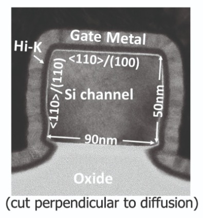
Figure 10. Intel’s monolithic three-dimensional layer transfer process flow involves the transfer of a layer of single crystalline silicon from a 300 mm silicon (100) donor wafer onto a completed 300 mm GaN-on-silicon (111) wafer, prior to fabrication of the top silicon PMOS transistors.

Figure 11. The cross-section of the top silicon PMOS transistor showing its finfet architecture, crystal orientation and current-carrying direction to boost hole mobility and performance. These silicon transistor design and architectural choices can be made independent of the choices made for the bottom GaN transistors.
Our monolithic three-dimensional stacking of GaN NMOS and silicon PMOS transistors provides a powerful way to integrate two dissimilar best-in-class semiconductor technologies on the same wafer and deliver the best performance, increased density, and greater functionality.
This technology has tremendous promise as it could enable entirely new classes of products with game-changing capabilities. Many exciting opportunities lie ahead, including the full integration of efficient, high-performance RF and power delivery with standard silicon-based processors. Such a technology has the potential to meet the demands of next-generation mobile devices, data infrastructure and communication networks for 5G and beyond.
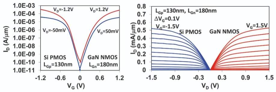
Figure 12. Current-voltage characteristics of the top layer channel length (LG is 130 nm) silicon PMOS transistor and the bottom channel length (LG 180 nm) GaN NMOS transistors. Dimensions have been chosen independently, to match drive current strengths and off-state leakages.
Thanks to its wide bandgap, GaN has vastly superior Johnson and Baliga figure-of-merits when compared with GaAs and silicon (see Table 1). These virtues enable GaN to operate at high frequencies and high power.
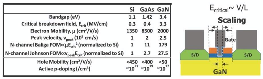
Table 1. Intrinsic semiconductor properties and figure-of-merits (FOM) for silicon, GaAs and GaN. N-channel GaN has the highest Baliga and Johnson FOMs, but P-channel GaN remains challenging due to low active p-doping and low hole mobility. The silicon PMOS transistor has a proven complementary P-channel with high hole mobility and high active p-doping.
An additional strength of GaN stems from the spontaneous and piezoelectric polarization effects associated with this family of materials. Due to this, a two-dimensional electron gas is produced in the GaN channel at the interface of GaN and a related ternary alloy, without the need for impurity doping.The resulting GaN heterostructure has a high carrier concentration, and also a high electron mobility, due to the low effective mass of the electrons and the absence of impurity scattering.
Yet another strength of GaN is that, due to its wide bandgap, it has a critical breakdown field that is at least ten times that for GaAs and silicon. This allows GaN transistors to be scaled to smaller lengths, leading to a higher performance. For example, for a supply voltage of 3.7 V, which is that provided by a lithium-ion battery, GaN transistors can be shorter, have a lower resistance and provide a higher drive current. Strengths such as these have made GaN the best semiconductor technology in production today for power and RF performance.
H. W. Then et al. “3D heterogeneous integration of high performance high-κ metal gate GaN NMOS and Si PMOS transistors on 300mm high-resistivity Si substrate for energy-efficient and compact power delivery, RF (5G and beyond) and SoC applications”, IEDM, 2019.
H. W. Then et al. ““High-Performance Low-Leakage Enhancement-Mode High-κ Dielectric GaN MOS-HEMTs for Energy-Efficient, Compact Voltage Regulators and RF Power Amplifiers for Low-Power Mobile SoCs”, VLSI Technology Symposium, 2015.
S. Bader et al. “GaN/AlN Schottky-gate p-channel HFETs with InGaN contacts and 100mA/mm on-current”, IEDM, 2019.
N. Chowdhury et al. “First Demonstration of a Self-Aligned GaN p-FET”, IEDM, 2019.


