

Gallium oxide’s glorious potential

Thanks to the promise of substrate manufacturing costs that are comparable to sapphire and an ultra-wide bandgap that aids performance, gallium oxide power devices have the potential to displace those made from SiC and GaN by delivering a better bang-per-buck, argues National Energy Renewable Laboratory’s Senior Engineer and Analyst Samantha Reese and Scientist, Andriy Zakutayev.
INTERVIEW BY RICHARD STEVENSON
Q: When we look at wide bandgap materials for power electronics, there are the middleweights – silicon carbide and gallium nitride, which are today’s success stories – and the ultra-wide bandgap heavyweights gallium oxide, diamond and aluminium nitride. Do you think aluminium nitride and diamond can have any success?
SR: I definitely don’t expect diamond to have much of an impact, due to its high cost. However, maybe these devices could be used on satellites, where cost is far less of an issue.
My impression from attending the recent SPIE Photonics West conferences is that AlN has some technical challenges, so I’m not sure it will be a success in power electronics, but it may be useful for optoelectronics.
Q: Do you see gallium oxide as a competitor to gallium nitride? Or to silicon carbide? Or both?
SR: I think gallium oxide can take on both, as we could get devices with a low cost. Gallium oxide could easily take on silicon carbide, due to this. Gallium nitride, which is behind silicon carbide in terms of commercialisation, operates at lower voltages, and is lower in cost. But if gallium oxide gets to market quickly, it could thwart gallium nitride before it is established.
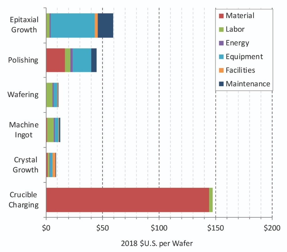
Figure 1. Ga2O3 wafer manufacturing cost by step
Q: Why does gallium oxide have the promise of low cost?SR: The cost of the device depends on the cost of the wafer. Silicon carbide is a hard material, requires expensive material for wafer production, such as diamond-based polishing slurries, thus it is expensive to make. Producing gallium oxide boules is very similar to producing those of sapphire, which is used to make LEDs. So gallium oxide promises low cost.
AZ: The bulk single crystal growth from melt also has other advantages compared to chemical processes that are not directly captured in substrate cost but may impact device cost – for example, a lower defect density of the wafer, and better yield for subsequent device fabrication.
Q: Do you view the wide bandgap as the greatest strength of gallium oxide?
AZ: The biggest merit in my opinion is the availability of large-size, high-quality, electrically-dopable bulk single crystal substrates with projected low cost. This is qualitatively different from silicon carbide and gallium nitride, or aluminium nitride and diamond; the width of the band gap is only a quantitative difference.
SR: Its other strength is its ability to work at high temperatures. This is useful for making sensors that go down deep wells. It could be used by the oil industry, which needs medium-voltage devices.
Q: One of the weaknesses of gallium oxide is its low thermal conductivity. Could that be a show stopper?
SR: That depends on who you talk to. Gallium oxide devices can be very small and thin, so you can use very effective thermal management, even though the thermal conductivity is so low.
At the recent IEEE Workshop on Wide Bandgap Power Devices and Applications, a paper given by a colleague of mine – Paul Paret from NREL in Golden, Colorado – showed thermal modelling of gallium oxide devices attached to a base plate. Because the base plate can be so large compared with the size of the device, there was no impact associated with the low thermal conductivity.
AZ: In real-world power electronics systems, the overall thermal resistance is often limited not by the thermal conductivity of the substrate, but by the thermal resistance of various interfaces between the semiconductor chip and other components. So low thermal conductivity of gallium oxide may be not as big a problem as often perceived. Also it depends on the use – power electronics versus RF devices versus a myriad of other potential applications – and some are more sensitive to this problem than others.
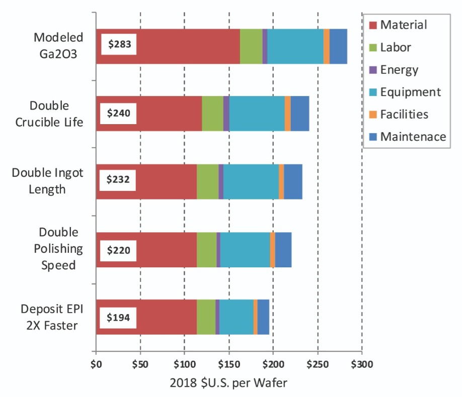
Figure 2. Ga2O3 Wafer Manufacturing Potential Cost Reduction Pathway
Q: Is the lack of p-doping for gallium oxide a big issue?AZ: It is an issue for traditional device designs, but also an opportunity for creating thinking. For example, enhancement-mode – that is, normally-off – gallium oxide vertical transistors with breakdown voltage of more than a kilovolt have been demonstrated without p-type doping, using a FinFET-like structure, by a team led by researchers at Cornell.
Q: You have modelled the costs associated with producing gallium oxide devices. Tell me about the assumptions you make, and how they are justified.
SR: I modelled the cost of the gallium oxide wafer with an epilayer, and stopped at the wafer level. However, I think that the cost of making a device from a wafer could be similar for gallium oxide and silicon carbide.
The cost of producing gallium oxide is dominated by the iridium crucible. We have been very conservative in calculating this cost, assigning the number of times that it could be re-used to sources that were credible. We are confident that that it can be re-used ten times, however there were anecdotal references in literature that it could be re-used considerably more or refurbished without significant cost.
We have assumed that all the equipment for making the wafers has had to be bought new, and that there are no subsidies for the manufacturer. We also assume that the equipment is running all the time, apart from downtime for maintenance. Obviously, if you only make one or two gallium oxide wafers per month, it is going to be prohibitively expensive.
Another assumption that we made is that the gallium oxide wafers are 6-inch. Today they are commercially available in 2-inch or 4-inch, and 6-inch are in a development process, but we have used 6-inch in our modelling because we want an apples-to-apples comparison with the published silicon carbide cost.
Q: What were your key findings, in terms of wafer costs?
SR: Our figures are based on current material quotes for gallium oxide powder. If production took off, costs could come down, as there is not much of a market for gallium oxide powder today. With the stated assumptions, we find that the cost of gallium oxide is three times lower than silicon carbide, and with improvements could be five times less expensive. Additionally, gallium oxide wafer manufacturing could benefit from the expertise already gained in manufacturing of sapphire wafers.
Q: Why are the iridium crucibles so expensive?
SR: Iridium is a rare and expensive material. It’s not due to high processing costs for producing the crucible.
Q: Your work shows that the cost of a 6-inch gallium oxide wafer could be just under $300 – that’s a third of that for silicon carbide. That’s very encouraging. And you think it could be even lower than that. What are the most promising routes for getting the costs right down, and how big an impact could they have?
SR: The cost of the indium crucible could come down by 15 percent. If the size of the ingot were to double, this would provide an additional 3 percent saving. If the processing rate were to increase by 60 percent, then this could trim another 4 percent. A doubling of the growth rate could cut another 9 percent. If you put that all together, the cost of the wafer could come down from $300 to $200, a 33 percent reduction.
After that, replacing iridium with another metal would be the most promising transformative route.
Q: Novel Crystal Technology, a joint venture by Tamura Corporation and the National Institute of Information and Communications Technology, is producing gallium oxide material by two different methods. How do you think your findings relate to Novel Crystal’s production costs? Could there be differences due to economies of scale, and the maturity of the production process?
SR: I can’t comment on Novel Crystal Technology or other specific companies. However, at a conference one gallium oxide substrate maker indicated that their internal costs of production are very similar to those of our model, when they make the same assumptions. This is the best validation of our work we can get.
When companies produce just a few wafer per month, the manufacturing costs will be higher. But when you scale to volume, the costs will come down.
Q: Does a lower wafer cost directly translate into a lower bill-of-materials for a device?
SR: It is not a one-to-one scenario. There are other ‘fixed costs’. For about a three-fold reduction in the cost of the epi-wafer, the device would be about half as expensive, since the wafer is usually 60-to-70 percent of the cost of the device.
With wide bandgap devices, whether they are silicon carbide or gallium oxide, they can produce cost reductions at the system level, thanks to a reduction in the cost of the magnetics.
There is also an increase in the efficiency. Take a 50 kilowatt inverter, for example. Turning to gallium oxide devices might provide a 5 or 6 percent increase in efficiency, leading to a 2 percent increase in the electrical output from a solar farm, so an increase in revenue.
Q: Which company’s do you think will bring the first devices to market? Flosfia of Japan?
AZ: Our SPIE and Joule papers are about β-gallium oxide, which has a monoclinic structure. Flosfia is working on a-gallium oxide, which has a hexagonal ‘corundum’ structure that is similar to sapphire. That is a completely different technology. It’s not clear yet which company would emerge as a leader in β-gallium oxide devices.
Q: With silicon carbide, it took more than a decade to follow up the launch of the first Schottky barrier diode with the first MOSFET. With gallium oxide, do you expect diodes to launch first, followed by MOSFETs? And could the gap between them be a decade or more?
SR: I think it will probably be diodes first, but the wait for MOSFETs will be shorter than it has been for silicon carbide. That’s because silicon carbide has helped to pave the way for the commercialisation of gallium oxide. For example, contact layer sintering processes have been established, and there are high-temperature modules that gallium oxide devices can be designed into. The US Air Force Laboratory is very excited about gallium oxide. And if you look at the number of papers published in total, you can see that there is major interest in gallium oxide worldwide.
AZ: I agree that it is likely that gallium oxide Schottky barrier diodes will be commercialised first, because their fabrication technology is relatively straightforward. However, lateral radio-frequency transistors similar to gallium nitride may be commercialized sooner than vertical power transistors similar to silicon carbide.
SR: I can’t comment on Novel Crystal Technology or other specific companies. However, at a conference one gallium oxide substrate maker indicated that their internal costs of production are very similar to those of our model, when they make the same assumptions. This is the best validation of our work we can get.
When companies produce just a few wafer per month, the manufacturing costs will be higher. But when you scale to volume, the costs will come down.
Q: Does a lower wafer cost directly translate into a lower bill-of-materials for a device?
SR: It is not a one-to-one scenario. There are other ‘fixed costs’. For about a three-fold reduction in the cost of the epi-wafer, the device would be about half as expensive, since the wafer is usually 60-to-70 percent of the cost of the device.
With wide bandgap devices, whether they are silicon carbide or gallium oxide, they can produce cost reductions at the system level, thanks to a reduction in the cost of the magnetics.
There is also an increase in the efficiency. Take a 50 kilowatt inverter, for example. Turning to gallium oxide devices might provide a 5 or 6 percent increase in efficiency, leading to a 2 percent increase in the electrical output from a solar farm, so an increase in revenue.
Q: Which company’s do you think will bring the first devices to market? Flosfia of Japan?
AZ: Our SPIE and Joule papers are about b-gallium oxide, which has a monoclinic structure. Flosfia is working on a-gallium oxide, which has a hexagonal ‘corundum’ structure that is similar to sapphire. That is a completely different technology. It’s not clear yet which company would emerge as a leader in b-gallium oxide devices.
Q: With silicon carbide, it took more than a decade to follow up the launch of the first Schottky barrier diode with the first MOSFET. With gallium oxide, do you expect diodes to launch first, followed by MOSFETs? And could the gap between them be a decade or more?
SR: I think it will probably be diodes first, but the wait for MOSFETs will be shorter than it has been for silicon carbide. That’s because silicon carbide has helped to pave the way for the commercialisation of gallium oxide. For example, contact layer sintering processes have been established, and there are high-temperature modules that gallium oxide devices can be designed into. The US Air Force Laboratory is very excited about gallium oxide. And if you look at the number of papers published in total, you can see that there is major interest in gallium oxide worldwide.
AZ: I agree that it is likely that gallium oxide Schottky barrier diodes will be commercialised first, because their fabrication technology is relatively straightforward. However, lateral radio-frequency transistors similar to gallium nitride may be commercialized sooner than vertical power transistors similar to silicon carbide.
P. Paret et al. “Thermal and Thermomechanical Modeling to Design a Gallium Oxide Power Electronics Package.” 2018 IEEE 6th Workshop on Wide Bandgap Power Devices and Applications (WiPDA). IEEE, 2019
Z. Hu et al. “Enhancement-mode Ga2O3 vertical transistors with breakdown voltage> 1 kV.” IEEE Electron Dev. Lett. 39 869 (2018)
S. Reese et al. “Regional Manufacturing Cost Structures and Supply Chain Considerations for Medium Voltage Silicon Carbide Power Applications.” ASME 2018 13th International Manufacturing Science and Engineering Conference. https://asmedigitalcollection.asme.org/MSEC/proceedings-abstract/MSEC2018/51364/V002T07A004/277049
Singh et al. “Performance and Techno-Economic Evaluation of a Three-Phase, 50-kW SiC-Based PV Inverter” [DOI: 10.1109/PVSC40753.2019.8980752]
S. Reese et al. “How Much Will Gallium Oxide Power Electronics Cost?” Joule 3 903 (2019) https://doi.org/10.1016/j.joule.2019.01.011
S. Reese et al. “Gallium oxide techno-economic analysis for the wide bandgap semiconductor market.” In Oxide-based Materials and Devices XI 11281 p. 112810H. International Society for Optics and Photonics, 2020. https://doi.org/10.1117/12.2565975


