

Helping gallium oxide keep its cool
Gallium oxide MOSFETs run at lower temperatures and switch better when they are transferred to substrates with a higher thermal conductivity.
BY Wenhui Xu, YiBo Wang, Tiangui You, Genquan Han and Xin Ou from SIMIT CAS and Xidian University
In recent years there has been much interest in gallium oxide. The form known as β-Ga2O3 has great promise for high-power devices, thanks to its combination of excellent electrical properties, adjustable doping and the potential for low production costs.
However, before this class of device can take on the likes of SiC and GaN, two significant hurdles must be overcome. One is the low thermal conductivity, which is only one-tenth of that of SiC, and is to blame for the self-heating and ultimately the poor performance of power devices. And the other is the absence of p-type doping, which prevents the production of p-n junctions that hold the key to realising low turn-on voltages and ultra-high breakdown voltages.
It is well accepted that the issue of thermal management could be addressed by heterogeneously integrating Ga2O3 onto a high thermal conductivity substrate, such as silicon or SiC (see Figure 1). But what growth technologies can be used to realise high-quality Ga2O3 thin films on these foundations? Many researchers have tried and failed to grow thin films of Ga2O3 on silicon and SiC heteroepitaxially. Polycrystalline Ga2O3 results, due to the large lattice mismatch with the substrate.
An alternative approach is to use the (100) cleavage plane of Ga2O3 to transfer micrometre-sized pieces to silicon, SiC or diamond. This is successful, but the small size hampers the commercial application of this technology.
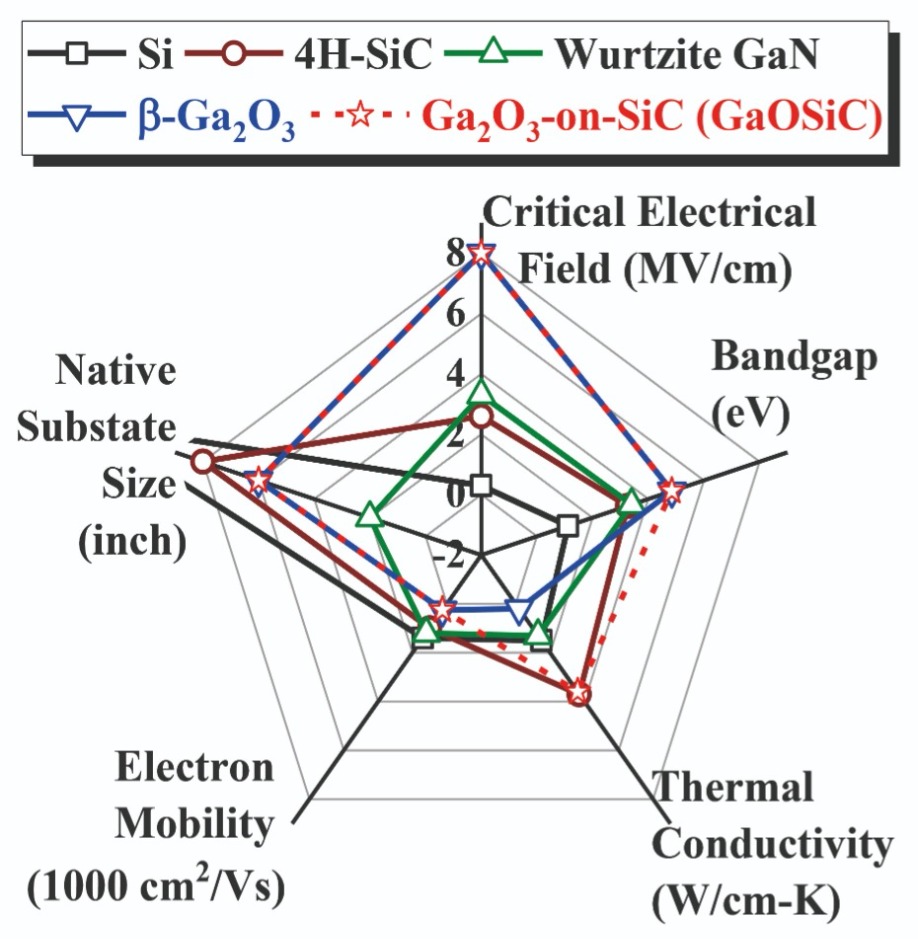
Figure 1. Ga2O3 has many material properties that are well-suited to power devices. k of Ga2O3-on-SiC (GaOSiC) is equal to that of SiC.
Yet another way forward is to use ion-cutting and wafer bonding techniques to transfer wafer-scale Ga2O3 thin films onto a high thermal conductivity substrate made from SiC or silicon. This is the approach being pioneered by our team, a collaboration between Xin Ou’s group in SIMIT, CAS, and Genquan Han’s group at Xidian University.This approach has much promise for high-volume manufacture, given that ion-cutting and wafer bonding are used for the mass production of silicon-on-insulator wafers.
Drawing on our experience with these processing techniques, we have obtained an appropriate implantation fluence for H+ and He+ in Ga2O3 bulk. This is of vital importance for forming the micro-cracks, which are key to exfoliating Ga2O3 films.
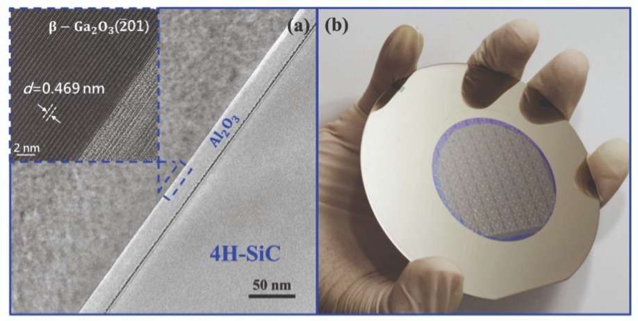
Figure 2. (a) Cross-sectional transmission electron microscopy of Ga2O3-Al2O3-SiC (GaOISiC). Inset shows the high-resolution transmission electron microscopy image of a single-crystalline β-Ga2O3 thin film on Al2O3. (b) MOSFETs on wafer-scale GaOISi.
Wafer bonding is a key step of the ion-cutting process. To strengthen this bond, we use a unique surface-activated bonding method, followed by a low-temperature annealing step. During the latter process, which is necessary for the exfoliation of Ga2O3 thin films from the implanted Ga2O3 wafers, there is a possibility that problems could arise, associated with the large thermal mismatch between Ga2O3 and the high-thermal-conductivity substrates. We have thoroughly investigated this, before optimising our process to prevent the debonding caused by thermal stress. Using the improved implantation and annealing processes, we have successfully transferred 400 nm-thick, 2-inch (201) Ga2O3 films onto SiC and silicon substrates. To thoroughly evaluate this process, we have fabricated MOSFETs on the resulting structure and measured their performance (see Figure 2).Note that we employ an additional post-annealing process to improve the quality of the transferred Ga2O3 thin films. This step narrows the peak of the X-ray diffraction rocking curve – the full width at half-maximum shrinks from 280 arcsec to 140 arcsec. In addition, we use a chemical-mechanical polish to extricate an implantation-induced damage layer close to the top surface. This step reduces the surface roughness of the transferred Ga2O3 thin films to just 0.4 nm.
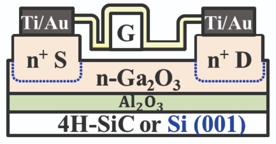
Figure 3. The architecture of the Ga2O3/Al2O3/SiC(Si) MOSFET.
Making MOSFETsOn this template we have made a trench MOSFET, realising E-mode operation by varying the channel thickness (see Figure 3). When it is much less than 40 nm, the transistor is normally off, due to the interface states between Ga2O3 and the gate dielectric that depletes the carriers in the channel.
To lower the contact resistance, we turned to source and drain implantation. This reduced the specific on-resistance to 49 mΩ cm2. We have also added a field-plate structure, which has increased the breakdown voltage to 800 V (see Figure 4). An even higher value can be obtained by eliminating interface defects, plus those that are induced by ion implantation.
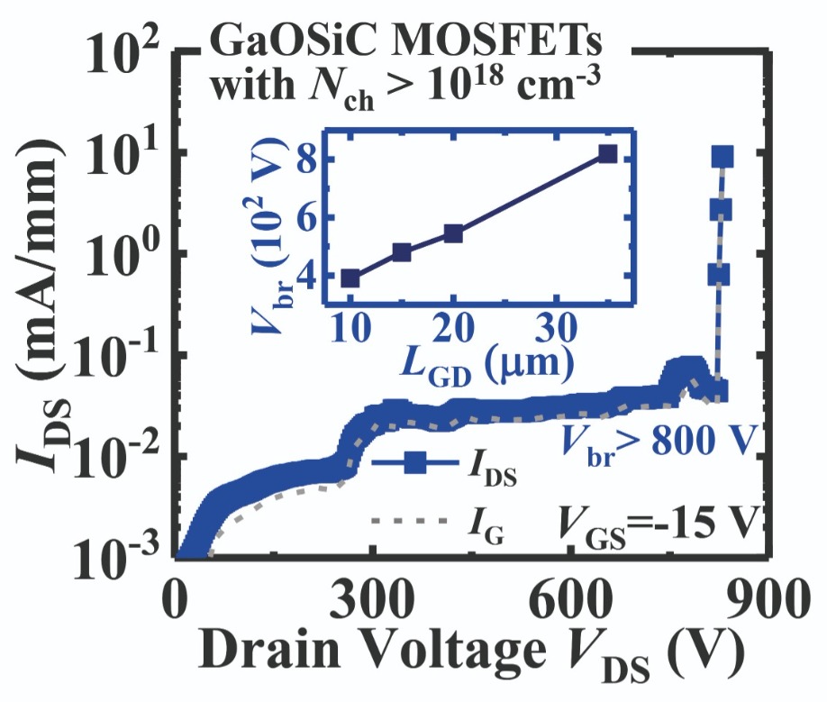
Figure 4. Three-terminal breakdown measurement of GaOSiC MOSFETs with a field plate. The inset show the breakdown voltage (Vbr) as a function of gate-to-drain spacing for separations up to 35 μm.
We have assessed the thermal stability of both our Ga2O3-Al2O3-SiC and Ga2O3-Al2O3-silicon MOSFETs using measurements of the temperature-dependent electrical performance (see Figure 5). Plots of the drain current as a function of drain voltage reveal remarkable thermal stability.Our analysis of the thermal stability of our fabricated MOSFETs has included simulations. As expected, they show that the operating temperature of the device on a SiC substrate is smaller than that on the Ga2O3 bulk substrate. According to transient thermal reflection measurements, the thermal conductivity of Ga2O3-Al2O3-SiC is very close to that of SiC, and significantly higher than bulk Ga2O3.
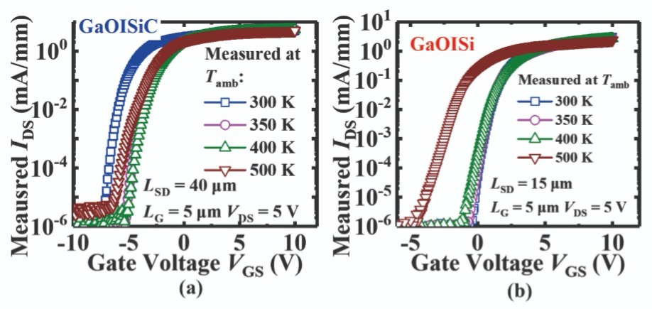
Figure 5. Transfer characteristics of GaOISiC and GaOISi MOSFETs measured at different temperatures.
Another benefit of the high thermal conductivity substrate is an increase in the temperature-dependent current ratio between the on-state and the off-state. When the temperature increases from 300 K to 500 K, the on-off ratio for Ga2O3 MOSFETs on SiC and silicon decreases by only an order of magnitude, while for equivalent devices on bulk Ga2O3 this figure falls by more than five orders of magnitude (See Figure 6 (a)).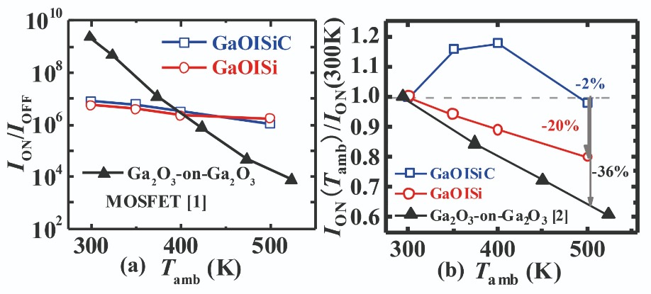
Figure 6. (a) On-off ratios show very little variation with temperature in GaOISiC and GaOISi MOSFETs, but do in Ga2O3-on-Ga2O3 devices. (b) As the ambient temperature (Tamb) increases to 500 K, GaOISiC and GaOISi MOSFETs show a 14 percent increase in on-resistance (Ron), a figure far lower than that of a Ga2O3-on-Ga2O3 device. Reference [1]: M. H. Wong et al. IEEE Electron Device Lett. 37 212 (2016). [2]: M. H. Wong et al. Appl. Phys. Lett. 109 193503 (2016).
To identify the primary culprit for the drastic decline with increasing temperature for the on-off ratio of Ga2O3 MOSFETs on native substrates, we investigated how the on-state current varies with temperature. This revealed that the on-state is not the largest contributor to the drastic decline that comes from self-heating (see Figure 6(b)). Instead, it is the off-state current.It is well known that self-heating effects are generally not observed in the off-state, due to minimal power dissipation in the devices. The addition of an Al2O3 insulator between Ga2O3 and a silicon or SiC handle leads to a very stable off-state current. In comparison, in the devices with a foundation of bulk Ga2O3, as temperature rises there is a significant increase in the off-current, due to degradation of the insulating properties.
The production of a semi-insulating Ga2O3 substrate involves iron-compensation doping. This results in a high concentration of acceptor traps at the valence band. As temperature increases, traps release some of the electrons that are captured. The Ga2O3 remains weakly n-type, contributing to the increase in the off-current of the transistor. We have simulated the off-current distribution in different device designs, and our findings mirror the results obtained at room temperature and an elevated temperature (see Figure 7).
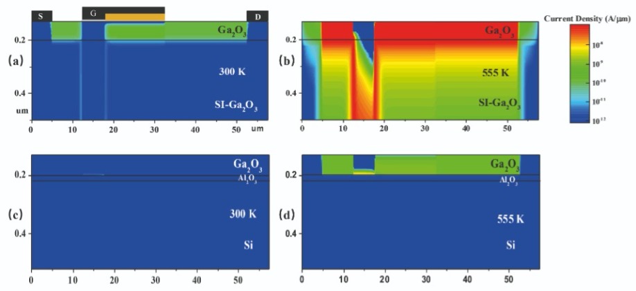
Figure 7. Simulations show a remarkable rise in the off-current at a drain-source voltage of 5 V in Ga2O3-on-Ga2O3 devices at 555 K compared with 300 K. (a) and (c) shows off-current distribution of Ga2O3-on-Ga2O3 and GaOISi at 300 K respectively; (b) and (d) show the off-current distribution of both structures at 555 K.
We are sure that our work has much promise. We have already demonstrated that heterogeneous integration improves the thermal stability of Ga2O3 MOSFETs and combats current leakage at high temperatures. As well as improving device performance, the use of ion-cutting and wafer bonding processes enable the reuse of bulk Ga2O3, driving down material costs. Our next step is to eliminate implantation-induced defects in the transferred Ga2O3 thin films, as this will take device performance to a new high. Such a move will take our industry another step closer to the emergence of Ga2O3 products for the power electronics industry.W. Xu et al. in IEDM Tech. Digest 2019 p. 12.5.1
Y. Xu et al. Ceram Int. 45 6552 (2019)


