

GaN HEMTs: The benefits of far higher voltages

Doubling the supply voltage of an RF GaN HEMT increases its power per die area and enables a substantial reduction in the size of very-high-power systems
By Sebastian Krause from the Fraunhofer Institute for Applied Solid State Physics IAF
Recently, GaN HEMT technologies have been adopted in a variety of applications, ranging from power conversion to mobile communication. This broad uptake has been spurred by the superior intrinsic material properties of GaN compared with competing silicon-based technologies. Thanks to the many merits of GaN, engineers can construct more efficient, smaller systems that trim operating expenses.
The rollout of 5G has taken interest in GaN to a new high. Initially it had been viewed as the best candidate for serving the 3 GHz to 6 GHz range, but more recently it has been tipped to also succeed in a millimetre-wave domain that spans 24 GHz to 39 GHz. Its virtues include a higher power density than conventional silicon LDMOS and silicon CMOS processes, enabling a reduction in chip size, which is a critical factor in multiple-input, multiple-output (MIMO) systems. In addition, as each GaN single chip die generates more power than its rivals, losses in off-chip power combining networks are reduced, leading to smaller, more efficient systems.
For the same reasons, GaN is found in a growing number of applications demanding a very high output power. For several years it has been successfully deployed in civil and military radar, and it is now a proven solution for powering these systems.
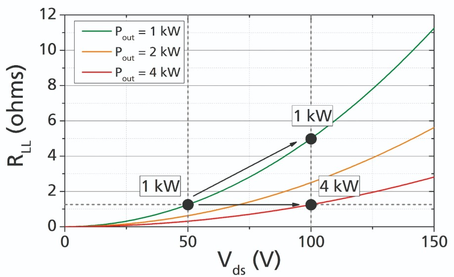
Figure 1. Load-line resistances of exemplary devices with output powers of 1 kW, 2 kW and 4 kW, plotted against supply voltage.
For these radar applications, one of the greatest attributes of GaN is its substantially higher efficiency than silicon LDMOS, its main rival in this field. Thanks to its higher efficiency, GaN dissipates less power, reducing the demand for air-cooling. What’s more, mirroring one of its strengths for wireless communication, GaN offers a superior power density over silicon LDMOS, leading to a higher power per die area. This attribute is particularly valued when scaling the output power towards multi-kilowatt levels. Here, a GaN-based system requires fewer devices for a given output power, simplifying system design. That’s not the only benefit, however – cutting component count also enables a substantial improvement in system resilience.Due to the numerous applications for GaN devices, during the last decade many different variants of this technology have been brought to market. Some processes, specifically developed for power conversion, are supporting supply voltages up to 1200 V. However, for technologies targeting RF applications, such as radar and telecom, voltages have been restricted to 28 V to 65 V. The main reason for this discrepancy is the difficulty in combining a high breakdown voltage with a good high-frequency performance. Improve on one front, and the tendency is to compromise on the other.
Minimising network losses
For very-high-power applications – such as pulsed and CW radar, particle accelerators, plasma generation and microwave heating – the workhorses are the established 50 V and 65 V GaN technologies, and 50 V silicon LDMOS. One of the biggest challenges in producing kilowatt amplifiers for these applications is matching them to the 50 W system impedance. Unfortunately, absolute output power is inversely proportional to load-line resistance, which may be thought of as the large-signal output resistance of a device. Consequently, as output power increases, load-line resistance falls. This makes life awkward for the circuit designer, often causing matching networks to become bulkier and more complex for very-high-power devices, and ultimately leading to higher network losses.
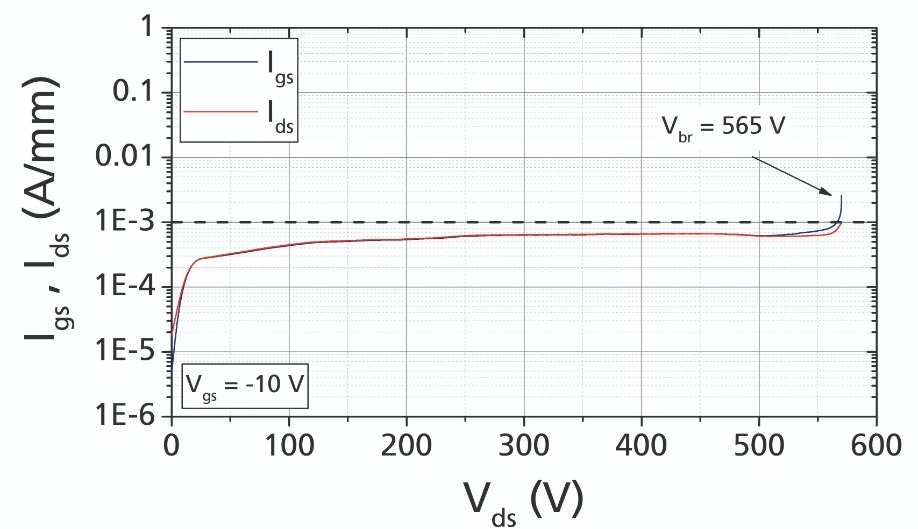
Figure 2. Breakdown voltage measurement of a Fraunhofer IAF 100 V GaN device with a 3.1 mm gate periphery.
One way to alleviate this issue to is to move to a higher supply voltage. Doing this inherently raises the load-line resistance of a device of given output power. In fact, there are two beneficial effects in play: the higher supply voltage leads to a proportionally higher power density; and, following from Ohm’s law, this results in an equal increase in load-line resistance. Thanks to the first of these benefits – the gain in power density – engineers can design devices with a smaller gate periphery for a given output power, leading to another hike in load-line resistance. Meanwhile, due to the second virtue, go through the maths and you’ll see that doubling the supply voltage of a device of a given output power ensures a four-fold increase in load-line resistance.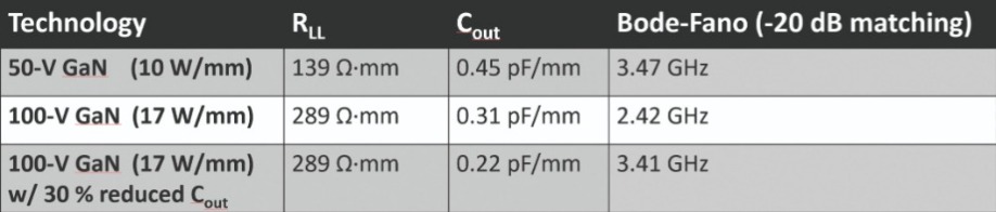
Table 1. Load-line resistance, output capacitance and resulting achievable bandwidth (Bode-Fano limit) for -20 dB matching of Fraunhofer IAF’s 50 V and 100 V GaN process, as well as a 100 V GaN process with reduced output capacitance.
Looking at this situation in a different way, it is now possible to employ an equally complex network, and therewith one that is similarly lossy, for a device delivering four times the output power. Due to this, it is easier to realise amplifiers with multi-kilowatt output powers.As all engineers know, there is no such thing as a free lunch. When the supply voltage increases, devices must withstand higher peak voltages, which occur under dynamic drive. To provide sufficient voltage robustness, engineers must ensure that the breakdown voltages of the RF devices that they employ are at least three-to-four times that of the operational voltage. So, for a device that is to deliver a reliable operation at 100 V, the breakdown should be in the 300 V to 400 V range. That’s not that far from the territory occupied by GaN devices designed for power electronics. However, those devices exhibit comparably large capacitances, limiting the suitable frequency range to just a few tens of megahertz. It is clear that the primary challenge when developing a 100 V GaN technology is to marry a high breakdown voltage with a suitable RF performance for the gigahertz range.
The key to increasing the breakdown voltage is to ensure appropriate control of the peak electrical field in the channel region while preventing the introduction of additional capacitances, which deteriorate RF performance. One possible measure is to increase the gate-to-drain spacing of the transistor. But this has major downsides – it increases the on-resistance of the device, and degrades its achievable output power density and maximum efficiency.
Our team at the Fraunhofer Institute for Applied Solid State Physics IAF is pursuing a more holistic approach, based on the combination of an increase in gate-to-drain spacing and optimisation of the source-terminated field plate. Efforts are directed at finding the best combination of breakdown voltage, on-resistance and output capacitance. As a high-voltage operation threatens to impair the long-term reliability of the device, from quite early in our development phase, we have been paying much attention to the origin of degradation mechanisms.
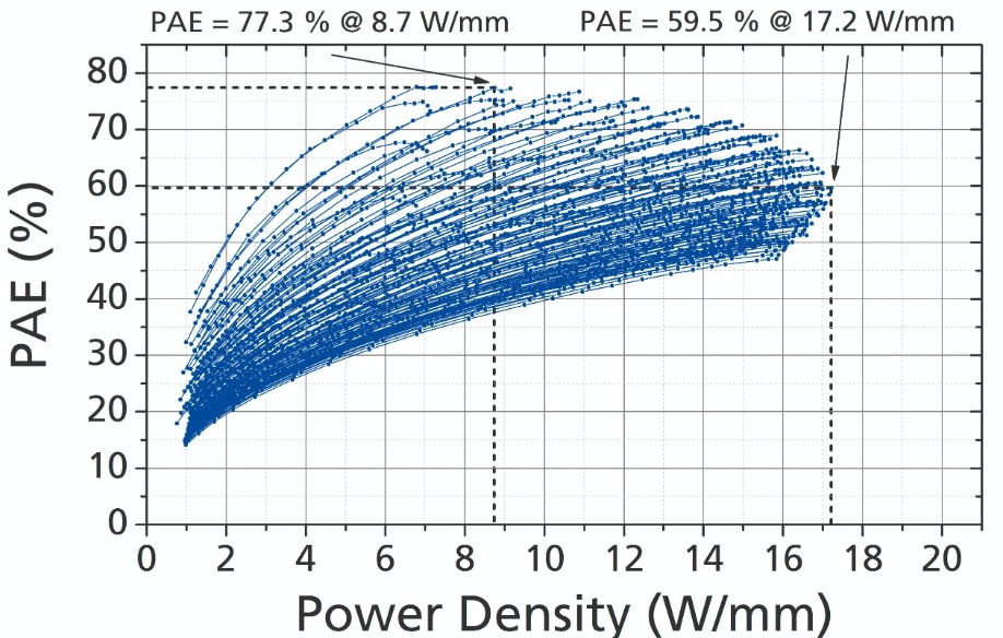
Figure 3. Pulsed 1.0 GHz load pull performance tests on a Fraunhofer IAF 100 V GaN device with 3.1 mm of gate periphery. Second and third harmonic output impedances have been terminated for maximum efficiency. Pulse width was set to 10 μs with a duty cycle of 10 percent.
Trading power for efficiency?One option for increasing the breakdown voltage is to extend the source-terminated field plate further towards the drain electrode, as this quashes the peak electrical field at the gate edge. The price to pay is an additional capacitance against the drain-side part of the channel. This manifests itself as additional output capacitance. For efficiency reasons, this additional extension of the field plate compared with a lower-voltage device should be kept as small as possible.
Usually, when an engineer designs a high-efficiency amplifier, they exploit a technique known as ‘harmonic termination’. Rather than matching just the fundamental frequency, they also use matching networks with specific impedances for the second and third harmonic frequencies – and sometimes even higher ones too. By taking this approach, they can design amplifiers operating in the likes of a Class-E, Class-F or Class-F-1 configuration that have a theoretical maximum efficiency of 100 percent. In comparison, the theoretical maximum for class B, involving shorting all harmonics, is just 78.5 percent.
When considering the behaviour of the HEMT, its helpful to think about the equivalent circuit. This is the combination of a load-line resistance and output capacitance that form a shunt RC-circuit. At high frequencies, the output capacitance dominates the output impedance of the transistor, resulting in a quasi-short-circuit. So, the higher the selected fundamental frequency, the greater the number of harmonics that tend to be intrinsically shorted by the presence of the output capacitance. This forces the device into a Class-B-like operation, limiting the theoretically achievable efficiency. To avoid this limitation and get the full benefit from the efficiency enhancement that harmonic termination brings, it is critical to ensure that the output capacitance is as small as possible.
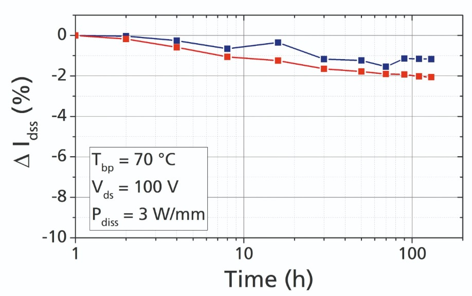
Figure 4. DC high-temperature operation lifetime results at a drain-source voltage of 100 V and a dissipated power of 3 W/mm of gate periphery. The baseplate temperature was set to 70 °C, resulting in a simulated junction temperature of 150 °C.
More power, less bandwidth?When designing an amplifier, one must note that the achievable bandwidth is inversely proportional to the product of load-line resistance and output capacitance – this is an outcome of the so-called Bode-Fano criterion. For example, if the load-line resistance doubles, the maximum achievable bandwidth halves. Note that the same relationship holds for a respective increase in output capacitance.
In principle, when the achievable bandwidth is lower, the network has to be more complex to match a given bandwidth. As stated before, a higher load-line resistance allows the use of simpler matching networks. However, this only holds when the achievable bandwidth is maintained. Consequently, the goal of the designer is to trim the overall output capacitance, so that this compensates for the higher load-line resistance caused by operation at a higher supply voltage.
Although a source-terminated field plate helps to reduce the peak electrical field in the channel, if it is poorly designed, it can impair device performance. As discussed already, when a source-terminated field plate is added, it creates an additional parasitic output capacitance. As the extra capacitance is detrimental to both the achievable efficiency and the matching bandwidth, it must be designed with much care.
Producing high powers
Building on our baseline 50 V GaN technology, we have developed a 0.50 μm gate length AlGaN/GaN-on-SiC technology for 100 V operation. We have used this to make our devices that feature a dual field plate configuration and individual vias in each source region. Thanks to the high power density of this process, output powers can exceed 500 W per single transistor die. To cope with the high dissipation associated with operation at elevated supply voltages, we have used finite element modelling to optimise all layouts.
Based on all the considerations that we have discussed here, such as the gate-drain distance and the insertion of the source-terminated field plate, we have developed our transistor technology to co-optimise efficiency and breakdown voltage. Initially, our efforts focused on L-band frequencies (1 GHz – 2 GHz), but we are now working to extend the usable frequency range beyond 6 GHz. Our view is that a well-engineered 100 V technology could feature capacitance values – such as those for the gate-source, gate-drain, and drain-source – that are comparable with those of established 50 V technologies. Succeed on this front and our 100 V devices should be able to serve a similar frequency range.
Measurements of the DC performance of our 50 μm single-gate-finger device reveal a maximum transconductance of more than 280 mS/mm at a 10 V drain-source voltage. We selected a gate length of 0.50 μm to minimise short-channel effects. Its success is proven by a very low drain-induced barrier lowering – it is below 5 mV/V.
We have undertaken further characterisation of our technology using a larger device, which has a periphery of 3.1 mm. By finding an optimum combination of extended gate-drain distance and geometry of the source-terminated field plate, we have trimmed the on-resistance to just 5.0 Ω mm. What’s very encouraging is that this device has a gate-drain breakdown voltage exceeding 550 V, without any evident buffer leakage current. We can benchmark this device by considering its ratio of breakdown voltage and on-resistance. It has a figure-of-merit of 110 V / (Ω mm), which is around 50 percent higher than that demonstrated by previous 100 V GaN technologies.
To assess power performance and maximum efficiency of our technology, we have used this device for RF load pull measurements. For this evaluation, made at a frequency of 1.0 GHz, we terminated the second and third harmonic impedances to ensure maximum efficiency. Tests reveal a maximum power density of around 17.2 W/mm and a power-added efficiency of 77.3 percent, based on load pull measurements of 169 different fundamental impedances. Our power-added efficiency at L-band frequencies is the highest value that has ever been reported for a 100 V GaN technology.
In addition to a high level of performance, RF devices need to deliver good reliability under elevated temperatures to serve in high-power systems. To gain some insight into the long-term stability of our technology, we have performed DC high-temperature accelerated lifetime tests on two of our 3.1 mm devices, which we mounted onto a 1 mm-thick copper-molybdenum-copper carrier. We found that after 130 hours of stress at an estimated junction temperature of 150 °C the saturation drain current fell by just 2 percent, demonstrating the basic reliability of our 100 V technology. We are now undertaking a more thorough reliability investigation at higher junction temperatures.
Our measurements provide an insight of what it should be possible to achieve with a 100 V GaN technology. We are now building on our record-breaking efficiency at L-band frequencies, with efforts directed at extending the applicable frequency range towards the C-band (4 GHz – 6 GHz), and even beyond. To succeed, we will need to further reduce our output capacitance. Do this and our efficiency will increase even more, particularly at high frequencies. An additional, associated benefit will be an increase in achievable bandwidth, leading to high-bandwidth, high-power designs.
Based on the progress we have made, we have every reason to believe that our 100 V technology will extend the limits of what can be realised with this wide bandgap technology.
S. Krause et al. “High-Power-Density AlGaN/GaN Technology for 100-V Operation at L-Band Frequencies,” 2019 IEEE International Electron Devices Meeting (IEDM), San Francisco, CA, USA, 2019, pp. 17.4.1-17.4.4.
G. F. Formicone IEEE Trans. Semicond. Manuf. 31 440 (2018)
R. Leoni et al. “Raytheon high power density GaN technology,” 2017 IEEE Compound Semiconductor Integrated Circuit Symposium (CSICS), Miami, FL, 2017, pp. 1-4.


