
Aixtron and partners continue to push tandem cell efficiencies
Aixtron is working with the Fraunhofer Institute, the Technical University of Ilmenau, and the Philipps University of Marburg to increase efficiencies of III-V multi-junction solar cells grown directly on silicon
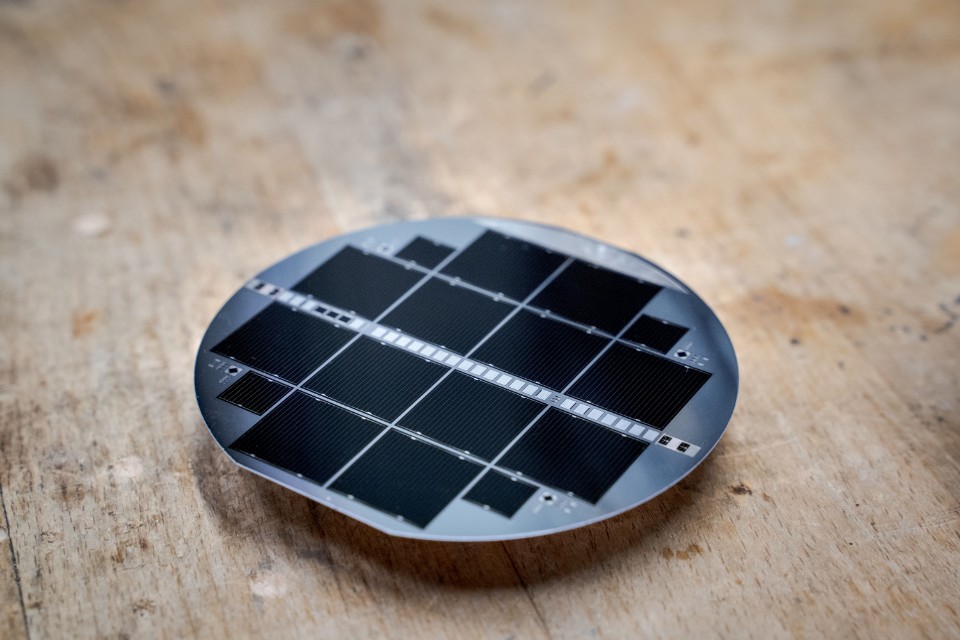
Aixtron has announced its involvement in a project that has so far achieved an efficiency of 25.9 percent with a multi-junction solar cell grown directly on a silicon substrate.
This figure was achieved by researchers at the Fraunhofer Institute for Solar Energy Systems ISE in close cooperation with the Technical University of Ilmenau, the Philipps University of Marburg and epitaxy experts at Aixtron SE, as part of the funded MehrSi project.
"For the first time we have now been able to realise a tandem solar cell based on a silicon wafer with such high efficiency," comments Dietmar Schmitz, VP corporate technology transfer at Aixtron. Until now, the production of III-V multi-junction solar cells has been based on a more expensive substrate material, for example also a compound semiconductor material.
Schmitz explains what is special about this basic research: "The gallium and phosphorus atoms must occupy the correct lattice positions at the interface with silicon. To achieve this, we have to control the atomic structure very well. This requires exceptionally high precision. In addition, to achieve the necessary high quality of the epi-wafers, it is crucial that a high crystal quality of all layers is achieved during epitaxial growth. This was achieved in the project thanks to the improved system technology developed by Aixtron and the good cooperation with the project partners".
In tandem photovoltaics, different combinations of high-performance solar cell materials are arranged in layers on top of each other in order to use the different wavelengths of sunlight more efficiently when converting light into electrical energy. Silicon is suitable for absorbing the infrared portion of the sunlight spectrum. Layers of different III-V semiconductor compounds, a few micrometers thick, are then applied to the silicon base to convert the ultraviolet, visible and near-infrared light more efficiently into electricity.
Work on faster crystal growth to further reduce manufacturing costs
Now the alliance partners are working to further increase efficiency and reduce manufacturing costs. To this end, the deposition of the layers is to be realised even faster, with higher throughput and thus more cost-optimised. In addition, the efficiency of the solar cells is to be further improved.
"Specifically, the dislocation density in the III-V solar cell layers is to be reduced from 108 cm-2 to the range of 1-5 x 106 cm-2 in order to increase the efficiencies to more than 30 percent. And last but not least, the cost-effectiveness of the epitaxy processes is to be further optimised," explains Michael Heuken, VP corporate R&D at Aixtron.
By means of more cost-effective processes in combination with silicon as the lowest sub-cell, tandem technology is to be made accessible for broad-based photovoltaics in the future. Aixtron has already been working on such III-V multi-junction solar cells on silicon with several partners for many years.
The project SiTaSol for the joint development of layer packages that can be produced as quickly and cheaply as possible is funded by the EU. In SiTaSol Aixtron has built and tested a specially optimised MOVPE system in its own laboratory.


