
Building better Gallium Oxide transistors
Wrapping modulation-doped Ga2O3 FETs in highly conductive materials addresses concerns related to thermal management and carrier transport
If Ga2O3 transistors are to fulfil their potential in RF and power electronics, issues must be addressed that relate to a low electron carrier mobility and heat extraction.Offering promising solutions to both these concerns is a US collaboration between engineers from The Pennsylvania State University, The Ohio State University, Kyma Technologies, Modern Microsystems and the University of Utah.
This team is making the case for replacing the MOSFET with a FET featuring modulated silicon δ-doping – a class of transistor known as the MODFET – and incorporating materials with a high thermal conductivity, to allow the device to run harder without overheating. Using the most capable architecture for heat extraction enables a five-fold increase in power handling.
Investigations by the team involved experimental studies and simulations. They included the use of thermo-reflectance thermal imaging to determine the surface temperature of the MODFET under various operating conditions. To validate those results, the engineers turned to nanoparticle-assisted Raman thermometry. Both techniques, which probed the temperature rise of the gate metal, gave excellent agreement. Values were replicated in simulations produced by Synopsys Sentaurus and COMSOL Multiphysics software.
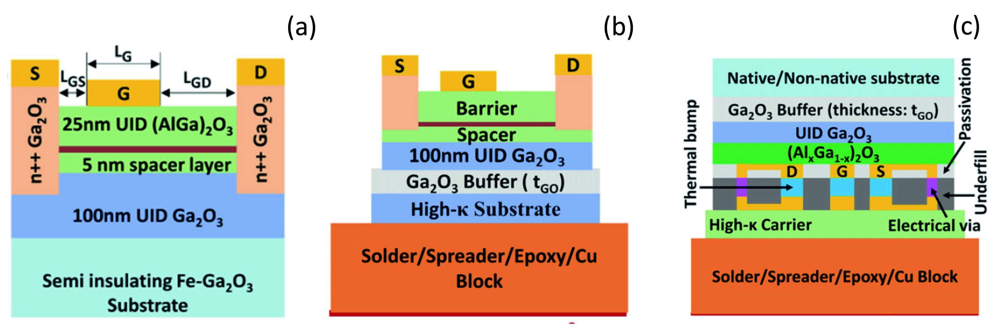
Simulations were employed to consider the impact of changes to gate-to-drain distance in MODFETs with a gate-to-source separation of 1 μm and a gate length of 3 μm (see Figure (a)). To increase the breakdown voltage in power FETs, designers tend to employ a gate-to-drain spacing that exceeds the gate-to-source separation. According to simulations, by increasing the gate-to-drain spacing from 3 μm – the distance used in the devices produced for the thermal measurements – to 20 μm slashed the peak electric field by an order of magnitude. In turn, the rise in peak temperature fell by almost 40 percent.
The engineers have also used simulations to consider the impact on power handling of the insertion of high thermal conductivity substrates underneath the MODFET. For a MODFET with a 10 μm-thick Ga2O3 buffer (see Figure (b)), mounting this device on a 4H-SiC wafer led to a reduction of 46 percent in the rise in maximum temperature. Replacing 4H-SiC with diamond, which has a thermal conductivity around four times higher, delivered further improvement. However, gains were modest, delivering just a 5 percent decrease in the maximum temperature, because the 10 μm-thick Ga2O3 buffer dominates the thermal dissipation of this device.
To evaluate the role that the buffer has on device heating when switching from 4H-SiC to diamond, the team also simulated MODFETs with Ga2O3 buffer thicknesses of 100 μm and 1 μm. For the former, diamond delivers only a 1 percent gain over 4H-SiC, but for the latter it is an improvement of 14 percent. However, the team is quick to point out that the feasibility of thinning a Ga2O3 buffer to just 1 μm is yet to be established.
Experimental verification of these trends came from infrared thermography measurements, supported by finite-element thermal modelling. The engineers demonstrated that the addition of a 500 μm-thick 4H-SiC wafer to MODFETs with a 10 μm-thick Ga2O3 buffer provided a 66 percent reduction in the peak temperature.
Further reductions in peak temperature can result from a double-sided cooling design. With this architecture, the best results come from a combination of: depositing nanocrystalline diamond over the FETs; using gold bumps, rather than those made from indium; and mounting the transistor on polycrystalline diamond.
Simulations suggest that for MODFETs operating with a channel temperature of 200degC, moving from the conventional homo-epitaxial design to an optimum double-sided design enables a hike in power density from 1.7 W/mm to 9.5 W/mm.
'Electro-thermal co-design of β-(AlxGa1-x)2O3/Ga2O3 modulation doped field effect transistors' by Chatterjee et al. Appl. Phys. Lett 117 153501 (2020)


