

Switching to silicon substrates for satellite communication

Today’s solid-state high-power power amplifiers operating in the microwave domain are based on the GaN-on-SiC HEMT. Replace the SiC with silicon and key attributes remain, while costs fall, thanks to production on larger wafers
BY ROCCO GIOFRÈ, FERDINANDO COSTANZO AND ERNESTO LIMITI FROM THE UNIVERSITY OF ROMA ‘TOR VERGATA’ AND ANTONINO MASSARI, FRANCESCO VITULLI AND ANDREA SURIANI FROM THALES ALENIA SPACE – ITALY
Broadband access services are destined for unprecedented growth this decade. As 5G is rolled out, data rates are climbing to 100 Gbit/s, while, in urban areas, simultaneous connections will total more than a million for every square kilometre. Alongside traditional services, such as video streaming, audio calls and data sharing, billions of daily used objects will be hooked up to the internet, including washing machines, fridges and ovens.
To underpin this new era in connectivity, there will need to be a new paradigm for the underlying network. This will include: a higher cell density, and thus a lower peak power; the introduction of a carrier frequency in the K-bands (18-27 GHz); an extended bandwidth; alternative channel access techniques, such as beam-division multiple access (BDMA); massive MIMO; and the use of more efficient spectrum aggregation signals. But even with all of this innovation, this network, which relies upon terrestrial infrastructures, will still fail to satisfy all of tomorrow’s requirements.
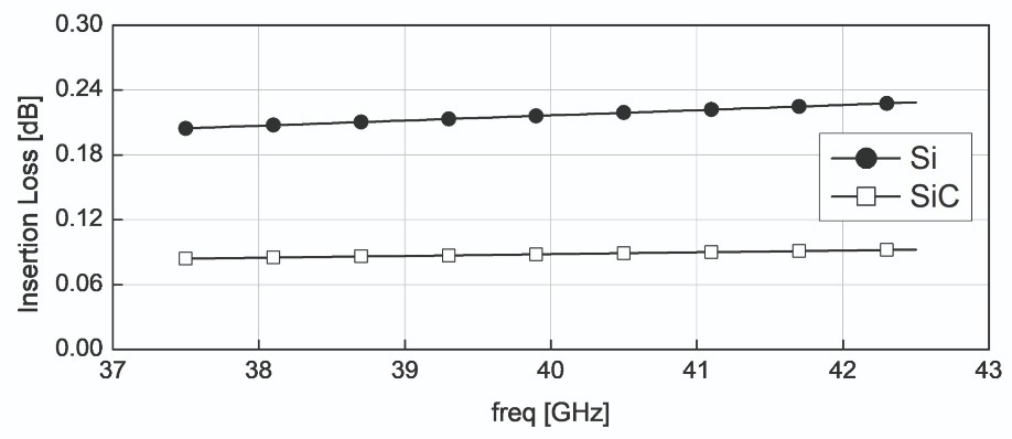
Figure 1. Simulated insertion loss of a transmission line with a Z0= 50 Ω characteristic impedance and 1 mm length realized on silicon (filled symbols) and SiC (empty symbols) substrates.
A key step in the deployment of very-high-throughput satellites is the development of high-performing space-borne equipment operating at high frequencies. It is envisaged that the feeder link, which is the radio channel between the satellite and a ground station, will be in the Q/V bands, so typically 40 GHz. Meanwhile the data link, providing the radio channel between the satellite and the end users, will reside in the Ka-band, at a frequency of 18.75 GHz.
Very-high-throughput satellites feature many beams. To accommodate this, satellites must house more equipment, realized ideally through miniaturization. New hardware needs to be lighter and smaller, as well as more reliable and better at thermal management.
Fulfilling all these requirements at the spacecraft level hinges on increasing the performance of the power amplifier, which sits at the last stage of the transmitting channel. This sub-unit of a payload consumes more than 75 percent of the overall DC power, so governs systems efficiency and thermal management requirements, while also impacting the reliability, mass and volume of the transmitter. In addition, the power amplifier determines the output power level and the spectral regrowth of the transmitted signal – these traits are determined by linearity and power characteristics.
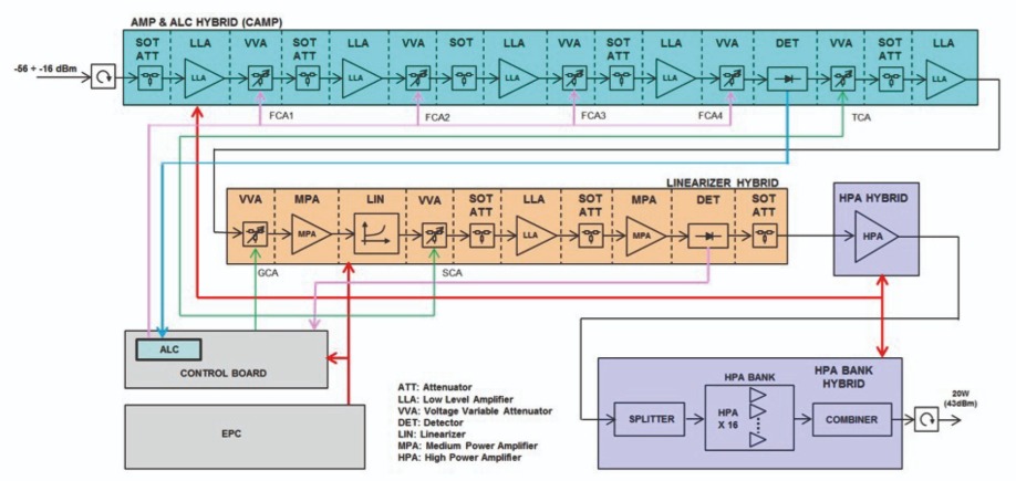
Figure 2. RF line-up of the solid-state power amplifier. It is composed by four sub-units, namely a Channel Amplifier (CAMP Hybrid), Linearizer Hybrid, HPA Hybrid and HPA Bank.
There are currently two types of process for producing GaN RF devices: one is for SiC substrates, and the other for silicon. The former has proven to be the best foundation for making high-power, efficient PAs at microwave frequencies, such as the Ku-band. However, silicon has much promise. This platform can exploit key features of most common GaN-on-SiC technologies, while drawing on additional benefits, including a reduced production cost, driven by larger wafers.
GaN-on-silicon: Concerns...
At this stage, doubts surround the suitability of GaN-on-silicon HEMTs for satellite communication. While studies have proven that GaN-on-SiC power amplifiers are a worthy replacement for tubes for several applications, the prospects for the GaN-on-silicon amplifier are held back by concerns related to thermal management and passive structure losses.
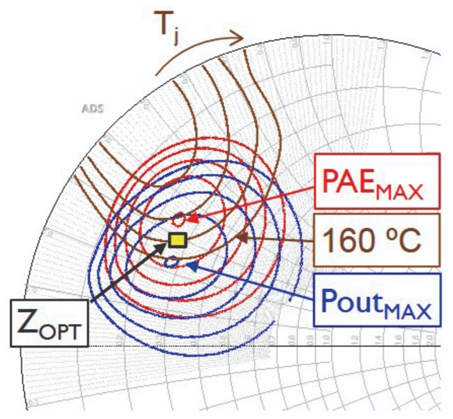
Figure 3. Simulated load-pull counters of the 4 x 75 μm device at a frequency of 40 GHz. Output power (blue), PAE (red), junction temperature (brown) and selected impedance (yellow).
To illustrate this, consider two 4 x 75 μm technologies, differing only in the substrate type (they have the same bias voltages, gain, power density, efficiency and so on). The GaN-SiC device produces an RF output power of 1.5 W, equating to a power density of 5 W/mm. The associated power-added efficiency is 50 percent, and the gain 10 dB. The performance is realised at a junction temperature below 160 °C, by restricting the base plate to 80 °C, conditions that lead to a power dissipation of 4.5 W/mm.
In comparison, the equivalent silicon device, having the same power-added efficiency, gain and periphery, has to operate at half the power density and power dissipation to ensure a junction temperature below 160 °C. To fulfil this requirement, the power density is limited to 2.5 W/mm, while power dissipation is around 2.25 W/mm.
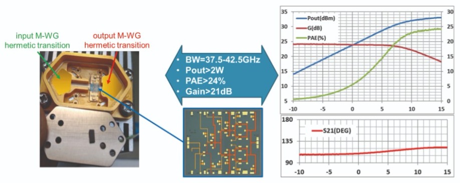
Figure 4. The assembled MMIC provides good performance at 40 GHz.
...and strengths
There are some remarkable advantages associated with GaN-on-silicon, including a lower material cost and access to larger wafers, which are well-suited to production volumes for 5G. By producing amplifiers from GaN-on-silicon, risks of import/export restrictions are diminished, making it easier to procure material.
And last but by no means least, GaN-on-silicon is compatible with heterogeneous integration in SiGe/CMOS technologies, so it offers many opportunities for making highly integrated, multi-functional chips.
To help drive adoption of the GaN-on-silicon power amplifiers in tomorrow’s communication satellites, our Italian collaboration – a partnership between researchers at the University of Rome ‘Tor Vergata’ and Thales – has built and characterised a Q-band GaN-on-silicon power amplifier. It features an RF tray, formed using a waveguide structure to combine sixteen MMIC power amplifiers realised with a commercial 100 nm gate length GaN-on-silicon process.
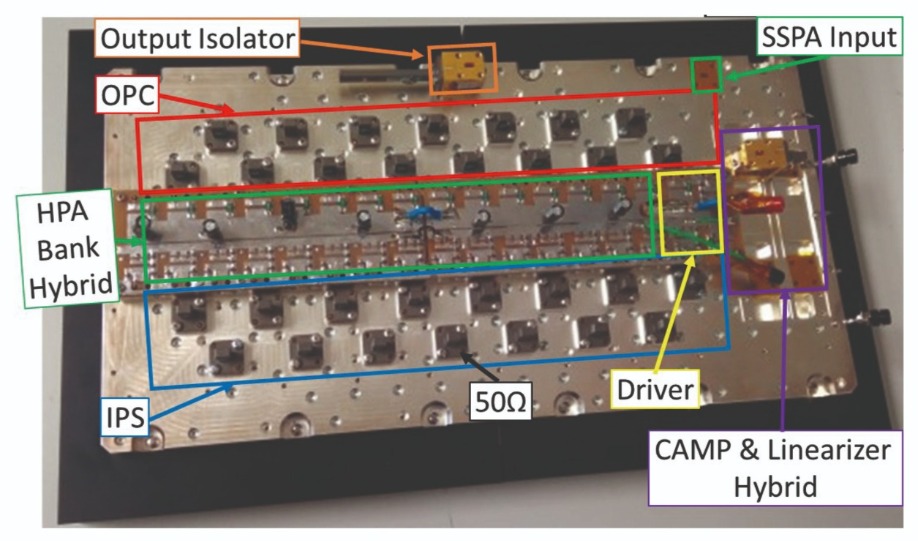
Figure 5. The splitter/combiner structures delivers an encouraging performance from 35 GHz to 45 GHz.
The first part of our power amplifier is the channel amplifier that provides an output of around -3 dBm. This sub-unit has a cascade of several low-level amplifiers and variable/fixed attenuators, carefully chosen to control the uplink flux, which can be adjusted by either ground telecommands – a fixed gain mode – or by an automatic level control loop. The latter is capable of compensating for in-orbit ageing of power amplifier gain, using a feedback signal provided by an integrated detector.
Downstream of the channel amplifier is a linearizer, primarily there to compensate for the nonlinearity of the high-power-amplifier bank that follows. The linearizer is designed to provide, as much as possible, equal but opposite amplitude-to-amplitude and amplitude-to-phase distortions with respect to those experienced by the high-power-amplifier bank.
Controlling the overlap between the expansion of the linearizer and the compression of the high-power-amplifier bank is a setpoint control attenuator. In this arrangement, the linearizer compensates for up to 7 dB of gain compression and +/- 45° of phase variation, and provides a constant output power of 7 dBm.
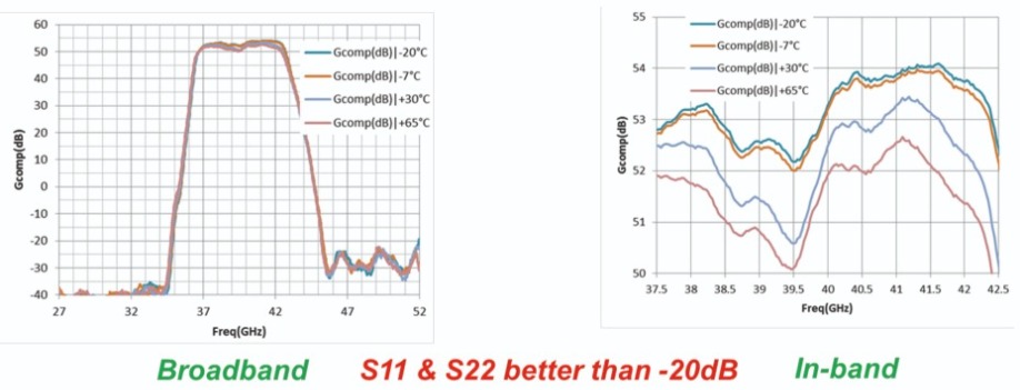
Figure 6. Measured small-signal performances of the solid-state power amplifier.
During the development of our MMIC, we devoted much effort to accounting for the thermal, electrical and physical constraints of GaN-on-silicon technology. This included undertaking a series of load-source pull simulations on devices with a different geometry, evaluated using the centre frequency, which is 40 GHz. For each geometry, as well as calculating the output power, power-added efficiency and gain, we considered the resulting junction temperature. For this work we assumed a base plate temperature of 80 °C, which corresponds to the maximum value expected below the MMIC.
For our load-pull simulations, we selected the optimum load impedance for the 4 x 75 μm device (the values for the output power, power-added efficiency, and junction temperature are shown in Figure 3). To ensure that we comply with the de-rating rules while maximizing the output power, we have selected a load impedance that is between those for maximum power and power-added efficiency, and we produce a junction temperature contour that is slightly lower than 160 °C. By adopting these conditions, we give ourselves a margin when implementing our actual MMIC. Although this choice sacrifices efficiency performance by about 1 percent, it guarantees fulfilment of the power level requirement at the circuit level.
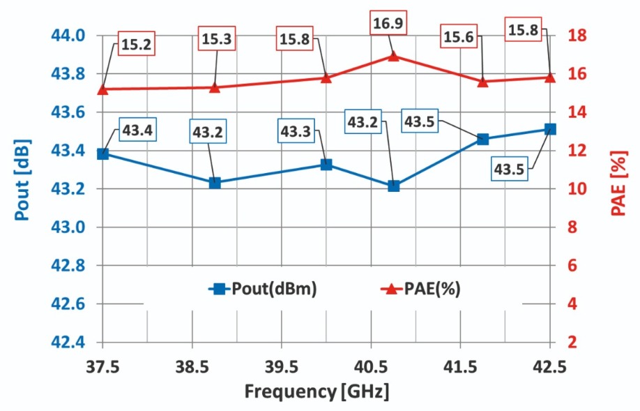
Figure 7. Measured large-signal performances of the solid-state power amplifier.
All of the MMICs used to form our power amplifier are equipped with an input and output microstrip-to-waveguide hermetic transition. This is visible in the picture of our MMIC, shown in Figure 4 alongside plots illustrating typical performance from 37.5 GHz to 42.5 GHz. Output exceeds 2 W, while the associated efficiency and gain are greater than 24 percent and 21 dB, respectively.
We have connected sixteen MMICs in the high-power-amplifier bank using a WR-22 waveguide splitter/combiner network. In our design there are fifteen T-magic structures, with a response that has been carefully optimised to minimize losses while ensuring a matching better than 20 dB at all ports. A waveguide isolator is added at the output side to improve the matching of the high-power-amplifier bank. We have measured losses for both the splitter and the combiner of 0.8 dB, and 0.3 dB for the isolator, giving a loss for the network of 1.9 dB.
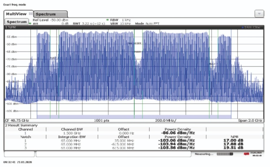
Figure 8. Measured noise-to-power (NPR) of the solid-state power amplifier (SSPA). This measurement was made by driving the SSPA with 301 uncorrelated carriers occupying a frequency band of 1.5 GHz large and applying three notches 65 MHz large.
For space applications, the thermal design of the amplifier is of upmost importance.
It is critical that the junction temperature of any active device does not exceed a safe figure for that particular technology, in order to guarantee reliable operation over the satellite lifetime, typically 15 years. For our amplifier, accurate thermal and mechanical design ensures that the hottest GaN-on-silicon MMIC never exceeds 160 °C, so long as the base plate temperature is no more than 65 °C.
Measurements of small-signal performance of our amplifier for base plate temperatures ranging from -20 °C to +65 °C, when the automatic level control loop is active, show that the forward voltage exceeds 53 dB, with a ripple lower than +/- 1dB in the overall operating bandwidth of 37.5 GHz to 42.5 GHz (see Figure 6). Input and output return losses are better than 20 dB, and gain variation over temperature is limited to less than 2 dB over 85 °C.
We have also measured our amplifier’s performance for a fixed gain of 65 dB at a base plate temperature of 65 °C. Saturated output power exceeds 20 W, with a power-added efficiency exceeding 15 percent, aided by a DC-DC converter efficiency of 90 percent (see Figure 7). Overall power consumption is 155 W at saturation, falling to 100 W for a 3 dB back-off, corresponding to a 10 W RF output power. Alongside efficiency, the linearity of a power amplifier is of paramount importance.
Linearity is critical in applications that include very-high-throughput satellites, which involve the use of time-varying envelope signals that feature a significant peak-to-average power ratio. We evaluate our linearity by measuring the noise-to-power ratio. This figure-of-merit, determined by driving our amplifier with hundreds of uncorrelated carriers, is 18 dBc (average) at an output power of +43 dBm (see Figure 8).
Our results compare well with other solid-state power-amplifiers, and highlight that GaN-on-silicon technology, despite its differences to GaN-on-SiC, can still yield high-performing power amplifiers in the Q-band for serving space applications.
Despite trailing travelling-wave tube amplifiers in efficiency – for the same power levels, they can hit 20 percent – our GaN-on-silicon-based design has a great deal to offer, combining a lower cost with graceful degradation and selectable form factor.
The upshot is a significant benefit for satellite designers.
The authors wish to acknowledge the Italian Space Agency (ASI) for funding this work in the context of project KALOS-DEVAQ within ESA’s ARTES C&G Technology Program. Particular thanks are due to Francois Deborgies from ESA/ESTEC for his expertise and technical support.


