

GaSb-based chips promise a sensing revolution
Compact spectroscopic infrared sensors could aid healthcare, farmers, and sportsman.
BY KRISTIJONAS VIZBARAS FROM BROLIS SENSOR TECHNOLOGY
Think of infrared chips and you’ll probably think of InP. That’s because this material and its related alloys have had tremendous success in this spectral domain, providing countless lasers and detectors for long-distance optical communication.
But InP can only get you so far. While it’s the number one choice in the near-infrared, if you want to go further in that direction while retaining inter-band transitions, you’ll need to consider another class of material. And providing the best choice is the GaSb system, which is paving the way towards an optical sensing revolution.
Merits of GaSb and its related alloys include an accessible spectral range spanning 1.5 µm to 4 µm – this is rich in strong, specific combinations of fundamental absorption bands associated with molecular rotational-vibrational transitions (see Table 1 for comparison). In addition, this material system enables high-volume, scalable manufacturing of efficient light sources and detectors that operate at room-temperature and can be integrated with SOI-based PICs.
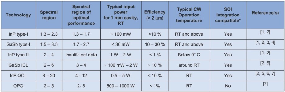
Table I. Comparing different technologies for infrared lasers underscores the merits of GaSb. [1] R. Wang et al. Sensors 17 1788 (2017) [2] S. Sprengel et al. Semicond. Sci. Technol. 31 113005 (2016) [3] K. Vizbaras et al. Proc. Of SPIE 8277 82771B, (2012) [4] K. Vizbaras et al. Appl. Phys. Lett. 107 011103 (2015) [5] A. Spott et al. IEEE Photonics Conference 2017, October 10, 2017 [6] M. Razeghi et al. Optics Express 23 8462 (2015) [7] M. Vitiello et al. Optics Express 23 5167 (2015)
Evaluating emission
For the GaSb material system – just as is the case for InP and its related materials – various options are available for generating laser emission. The most common is to use a type I quantum well, but for longer wavelengths interband cascade transitions may be needed. The pros and cons of these approaches, alongside alternative material systems, are outlined in Table 1.
Glance at this table and it is clear why the antimonide-based materials system is preferred, and why type-I technology is the best choice for high-volume applications that benefit from low energy consumption. Strengths include a mature design, high gain that results from the largest possible overlap between electron and hole wave-functions, and direct wafer-level testing of key electrical, optical and structural parameters – they include current-voltage characteristics, electroluminescence, and high-resolution X-ray diffraction spectra that offer an insight into strain, composition, and layer thickness. Having the opportunity to scrutinise a wafer before it is taped-in to make a device provides reliable early control of manufacturing yield, and allows pre-selection of wafers meeting the requirements to allow further processing.
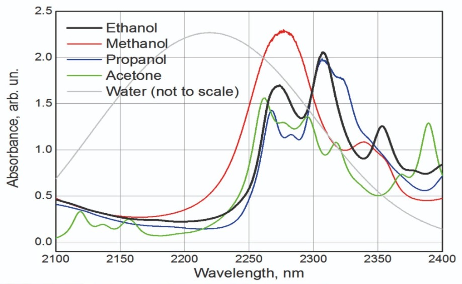
Figure 1. Infrared spectroscopy can identify ethanol, methanol, propanol and acetone by their unique absorbance spectra. The light grey line shows superimposed water transmission spectra.
For high-volume production of infrared and telecom-wavelength optoelectronic devices based on GaAs and InP, the most common substrate size is 3-inch. However, recent developments in datacom technology, primarily the roll-out of low-cost VCSELs, has led to an increase in the use of 6-inch GaAs substrates.

Table II. There are various of light source technology for accessing wavelengths beyond telecom. [1] K. Vizbaras et al. Appl. Phys. Lett. 107 011103 (2015) [2] R. Wang et al. Opt. Express. 24 28977 (2016) [3] R. Wang et al. Sensors 17 1788 2017 [4] S. Sprengel et al. Semicond. Sci. Technol. 31 113005 (2016) [5] K. Vizbaras et al. Proc. Of SPIE 8277 82771B (2012) [6] A. Spott et al. IEEE Photonics Conference 2017, October 10, 2017 [7] M. Razeghi et al. Optics Express 23 8462 (2015) [8] M. Vitiello et al. Optics Express 23 5167 (2015) [9] Cobolt Odin TM, IPG CLT-SF lasers (http://www.ipgphotonics.com/en/products/lasers/mid-ir-hybrid-lasers/1-8-3-4-micron/cl-sf-and-clt-sf-0-2-10-w http://www.coboltlasers.com/wp-content/uploads/2014/11/D0348-B_Datasheet-Cobolt-Odin-Series.pdf ).

Figure 2. The SOI part of Brolis’ widely-swept GaSb/SOI hybrid laser. Two coupled micro-rings are clearly visible.
Figure 3. Superimposed spectra show that four widely-swept GaSb/SOI lasers can cover the spectral range from 1900 nm to 2400 nm. Devices exhibit continuous-wave lasing with output powers of around 1 mW. As tuning involved only tuning a single micro-ring, spectral separation is defined by the free spectral range of a ring (several nm).
By working closely with MBE tool manufacturers, over the last eight years our team at Brolis has developed tremendous expertise and technology for multi-wafer, large-scale production of GaSb-based optoelectronic devices. Our first major milestone came in 2016, when we demonstrated the world’s first widely-swept hybrid GaSb/SOI laser. Since then we have made considerable progress in integrating GaSb type-I light emitters with SOI PICs.Our latest success is the fabrication of a GaSb-based monolithic laser spectrometer, based on four ultra-widely swept hybrid lasers and photodetectors. Lying at the heart of this spectrometer are four single-mode lasers, each with a side-mode suppression ratio exceeding 20 dB. These lasers are combined with two coupled micro-ring resonators with slightly different diameters, realised in an SOI circuit. By turning to the Vernier effect, we are able to electrothermally sweep the laser’s wavelength at a rate of up to 1 kHz. Each laser offers 120 nm of tuning, and by shifting the gain peak for each GaSb light source, we realise a combined tuning range of over 400 nm (see Figure 2).
If we thermally tune just one of the micro-rings, this leads to spectral hopping across the free spectral range of the ring – the mode hops are typically 4-5 nm. By tuning both micro-rings in a coordinated manner, we realise virtually quazi-continuous tuning across the entire spectral range (see Figures 3 and 4).
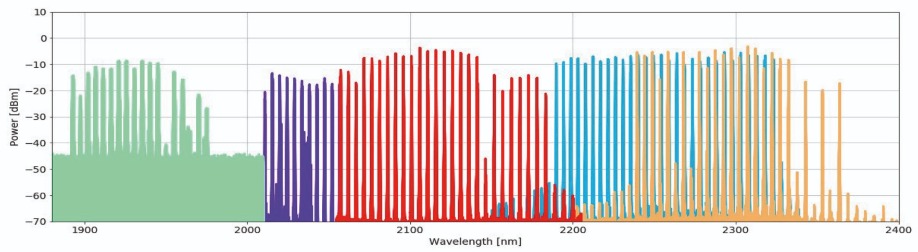
Figure 3. Superimposed spectra show that four widely-swept GaSb/SOI lasers can cover the spectral range from 1900 nm to 2400 nm. Devices exhibit continuous-wave lasing with output powers of around 1 mW. As tuning involved only tuning a single micro-ring, spectral separation is defined by the free spectral range of a ring (several nm).
As one may expect, our first hybrid sensor looked a little ‘clumsy’, as is often the case for new devices (see Figure 5 (a)). But it is functional, thanks to successful integration of four GaSb-based photodetectors, one GaSb-based light emitter and an external SOI cavity. Subsequent miniaturisation of this spectroscopic sensor is in progress (see Figures 5 (b) – 5 (c)), and it includes already 2-4 GaSb gain-chips, butt-coupled to the SOI and 4 GaSb control detectors flip-chipped on the SOI. The experimental tuning range (wavelength map) of one such hybrid device’s one channel is shown in Figure 3. In the long run, the technology should enable a footprint of just 2 x 3 x 1 mm, which is fully compatible with all current consumer and industrial platforms. Current sensor evaluation boards for internal use are shown in Figure 5 (c).

Figure 4. The peak wavelength of Brolis’ single widely-swept laser, when both micro-rings are electrothermally tuned in a specific manner. Continuous spectral coverage is clearly visible.
Multiple markets
The most famous application for spectroscopic sensing is measuring levels of glucose, an insight helping those with diabetes to monitor their condition. Realising this technology is not easy, because sensing glucose comes from measurements made on skin – that is, the tissue matrix – and this has great variability, both from person-to-person and from day-to-day. When those challenges are overcome, there is still the issue that glucose monitoring demands a highly regulated environment. Even if a technology is ready that addresses all these concerns, it could take up to a decade to enter the market.
A related field for transdermal spectroscopic sensors is monitoring lactates. One benefit of keeping track of lactate concentration in human blood is that a rise in value provides an early predictor of sepsis, which is responsible for one in five hospital deaths worldwide.
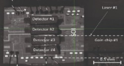

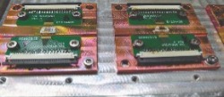
Figure 5. (left) Brolis first integrated GaSb/SOI sensor, based on four widely-swept lasers, has been produced in-house. On the lower right of the GaSb gain chip, the coupled to SOI external cavity is visible, along with: the four GaSb-based photodetectors flip-chipped on the SOI for wavelength control; output power monitoring (centre): and three additional ports for gain-chip coupling (the sides).(middle) Snapshot of current hybrid integration process – two GaSb gain chips butt-coupled to the SOI are visible. The automated hybrid integration robot is Brolis in-house designed and built. (right) Assembled BROLIS sensor demonstrators for evaluation boards (currently for in-house testing only). All four gain-chips, butt-coupled to the SOI are visible.
Another important molecule to consider is ethanol, key to measuring alcohol levels in the blood steam. It is possible to determine levels of ethanol by measuring the reflection spectrum through the skin (see Figure 6). This technique could curb accidents, due to the threat of exposing either drinking and driving, or drinking and working. In addition, it could help everyone to take more personal responsibility, by making self-monitoring available. It is far better to know that you have drunk too much to be safe to work or drive, than to be caught ‘in the act’, possibly after a fatality.
Uptake of a personal alcohol-monitoring system could be very high if such a device could be integrated in a wearable form or added to a wearable/smartwatch platform. Another option, available in the age of the IoT, is to integrate a sensor with a critical piece of machinery, such as a car or industrial tool. This could prevent intoxicated drivers from starting their cars, and operators under the influence of alcohol from using machinery.
Like the measurements of other molecules trans-dermally, it is a challenge to determine levels of ethanol. Success requires a long, expensive research and development effort, so it will be at least three-to-five years before a sensor will enter the market.
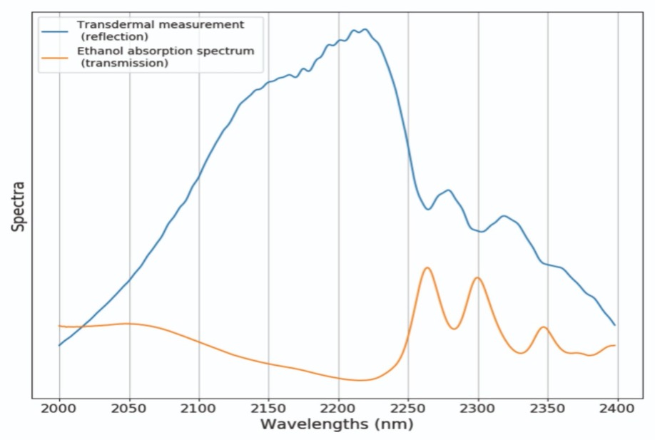
Figure 6. Transdermal optical signal of a tissue matrix containing ethanol, measured in reflection geometry (blue line) and ethanol absorption spectrum (orange). Characteristic ethanol absorption dips are clearly visible in the transdermal signal.
A related opportunity is the deployment of an ethanol content sensor in a fuel or another fluid matrix. This sensor could be handheld, or incorporated into existing industrial machinery.
Yet another potential application for GaSb-based sensors is the sorting of plastics, for recycling or other purposes. Different plastics can be identified by strong, clearly distinguishable features in the spectral range spanning 1.5 µm to 2.5 µm (see Figure 7). A laser spectrometer based on our technology offers a more affordable, compact alternative to the current solution, an expensive short-wave infrared camera.
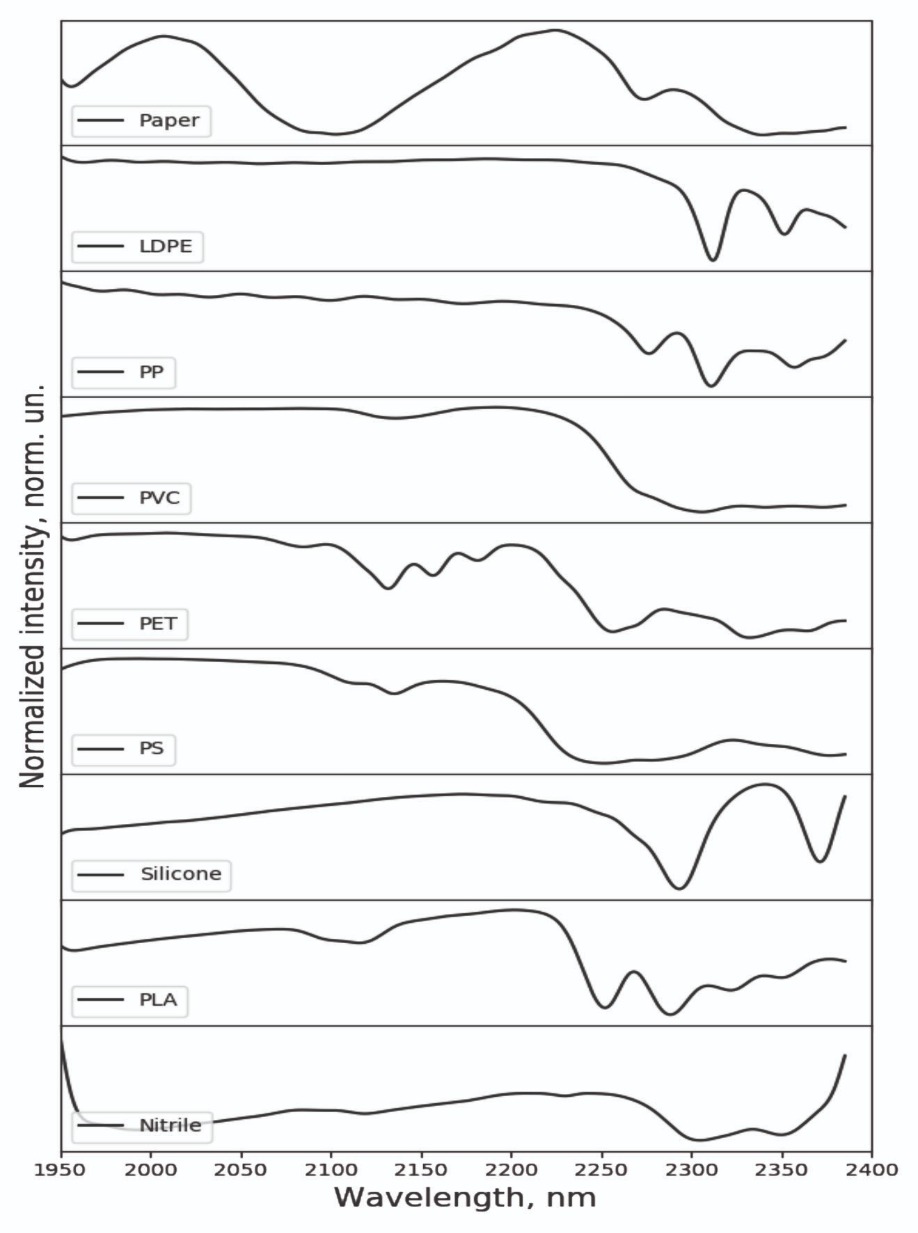
Figure 7. Sorting different types of plastic can draw on the transmission spectra of different materials.
Potentially lucrative opportunities for spectroscopic sensing also exist in the agricultural sector. This technology can identify milk constituents, such as fats, proteins, and urea, because they have significant absorption features between 1.5 µm and 2.5 µm. There is much merit in monitoring milk content in real-time and tracking trends in individual cows and their herds. If farmers monitor and record milk fat, milk protein, somatic cell count and urea content, they can adjust nutrition and get an early warning of incoming mastitis. Armed with this insight, they can take preventative action, rather than eventually prescribing antibiotics and removing the cow from milk production. With our technology, it should be easy to incorporate sensing hardware into most existing milking machinery.

The examples that we have listed here are just a fraction of those that exist for fluid, solid-state and gas sensing. The key point is that our current spectroscopic sensor – that is, our laser-spectrometer that combines widely-swept hybrid GaSb/SOI lasers with an uncooled GaSb-based detector on a single chip – is a powerful, generic piece of hardware that can address niche market segments and be scaled to serve consumer applications.


