
Powering underwater vehicles
Spacing thicker fingers closer together increase the conversion efficiency of GaInP power converters
Researchers at Chiba Institute of Technology, Japan, are claiming to have set a new benchmark for the performance of GaInP power converters. Their latest devices deliver a power conversion efficiency of 43 percent under illumination from a 638 nm laser at a power density of 17 W cm-2.
These GaInP devices are promising candidates for photo-receivers in optical wireless transmission systems powering autonomous underwater vehicles. For this application, lasers should emit in the range 400 nm to 700 nm, as this is where transmittance in sea water is high. That requirement rules out GaAs power converters; while they have an efficiency of over 80 percent between 825 nm to 850 nm, this falls to below 30 percent at wavelengths of 700 nm or less.
Last year the team reported the results of their first GaInP power converters incorporating a distributed Bragg reflector (DBR). Introduction of this reflector boosted power conversion efficiency to 43 percent, but only for irradiation densities below 3 W cm-2.
Significantly higher densities are needed for autonomous underwater vehicles. The team reasons that for a vehicle with a power consumption of 350 W, the laser’s power needs to be more than 1458 W, assuming an optical loss of 40 percent and a power conversion efficiency of 40 percent. And in that case, if the convertor cell has a 10 cm diameter, the laser intensity power density will need to be more than 11.1 W cm-2.
To develop a new generation of devices that work better in this regime, the team has investigated power converters that combine a DBR with better surface electrodes, which trim lateral spreading resistance.
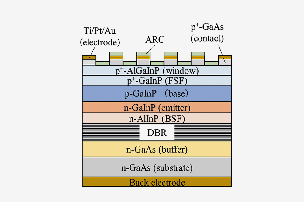
The engineers began by fabricating four GaInP power converter cells, all with dimensions of 2.4 mm by 2.4 mm (see figure above for details of the designs). This quartet included devices with and without a DBR that featured 12 µm-wide Ti/Pt/Au finger electrodes in a check pattern at a 485 µm pitch; and a pair of variants, featuring the same metal stack for the finger electrodes, but this time with an 11 µm width and a 115 µm pitch.
Measurements of the cells with a wider pitch showed that for a power density of around 0.1 W cm-2, the introduction of the DBR increased the conversion efficiency via a rise in open-circuit voltage. But at higher power densities these benefits were offset by Joule heat loss, due to increases in electrical and thermal resistance associated with the DBR.
Narrowing the pitch led to a significant improvement in the fill-factor and efficiency at high incident power densities. To reduce the lateral spreading resistance even further, the engineers increased the thickness of the AlGaInP window layer from 30 nm to 125 nm, and widened the front surface-field layer from 100 nm to 300 nm. With these additional refinements, devices with the 115 µm pitch produced an efficiency in excess of 43 percent from 2.8 W cm-2 to 17.1 W cm-2.
Although the fingers in these electrodes have a resistivity of just 4-6 x 10⁻⁸ Ωm, the resistance of one finger is as high as 9.6Ω, assuming a 1.0 mm length, a width of 11 µm and a thickness of 475 nm. Consequently, for the 12 parallel finger electrodes in the illuminated area, the total resistance is 0.8 Ω. To trim this resistance, the team increased the thickness of the fingers to 900 nm. This led to conversion efficiencies of 46.0 percent and approximately 45 percent under irradiation densities of 1.1 W cm-2 and 8.8 W cm-2, respectively.
Team spokesman Shiro Uchida says that even better results could come from an even smaller pitch, using thicker electrodes and adding more silver and gold into the electrode stack – this could reduce resistance.
'A 43.0% efficient GaInP photonic power converter with a distributed Bragg reflector under high-power 638 nm laser irradiation of 17 W cm-2' by Y. Komuro et al. Appl. Phys. Express 14 041004 (2021)


