
Simplifying measurements of low-level p-type doping in GaN
Photoluminescence spectra obtained at cryogenic temperatures unveil p-doping levels in GaN
Optimisation of the GaN MOSFET has been held back by difficulties in measuring the low levels of p-type doping employed in this power transistor. But this problem persists no longer, thanks to the work of a Japanese team from Oita University and Mirise Technologies. By using low-temperature photoluminescence measurements to unveil magnesium-based p-type doping levels over a very wide range, these researchers have trailblazed an alternative approach that is simple, non-destructive and non-contact.
While the cost of a low-temperature photoluminescence set-up is not insubstantial – the bill for a cryostat, spectrometer, detector and laser totals about $200,000 – it comes in at less than the alternatives, according to team spokesman Masato Omori from Oita University. He points out that conventional electrical measurement equipment, such as that based on the Hall effect, has a price tag of around $300,000, and says that it can cost more than $1 million to purchase device process equipment, used to form electrodes, etch material and dice wafers.
“In addition, wafers can be used directly in devices after the photoluminescence measurement,” argues Omori, “while wafers for electrical measurements are disposable and therefore wasteful.”
Another important consideration is that the process for forming an ohmic electrode with a low-concentration of p-type GaN – that is, less than 1 x 1018 cm-3 – is yet to be established. “The development of such technology requires a great deal of cost and time,” remarks Omori.
The technique that he and his co-workers have pioneered follows in the footsteps of Michio Tajima, who worked at the Japan Aerospace Exploration Agency in 1970s. During his time there, Tajima developed a method for quantifying the dopant concentration in silicon, based on considering the ratio of the intensity of the impurity-bound exciton line to the free exciton line. It is this ratio that Omori and co-workers are using to determine the magnesium acceptor concentration in GaN samples.
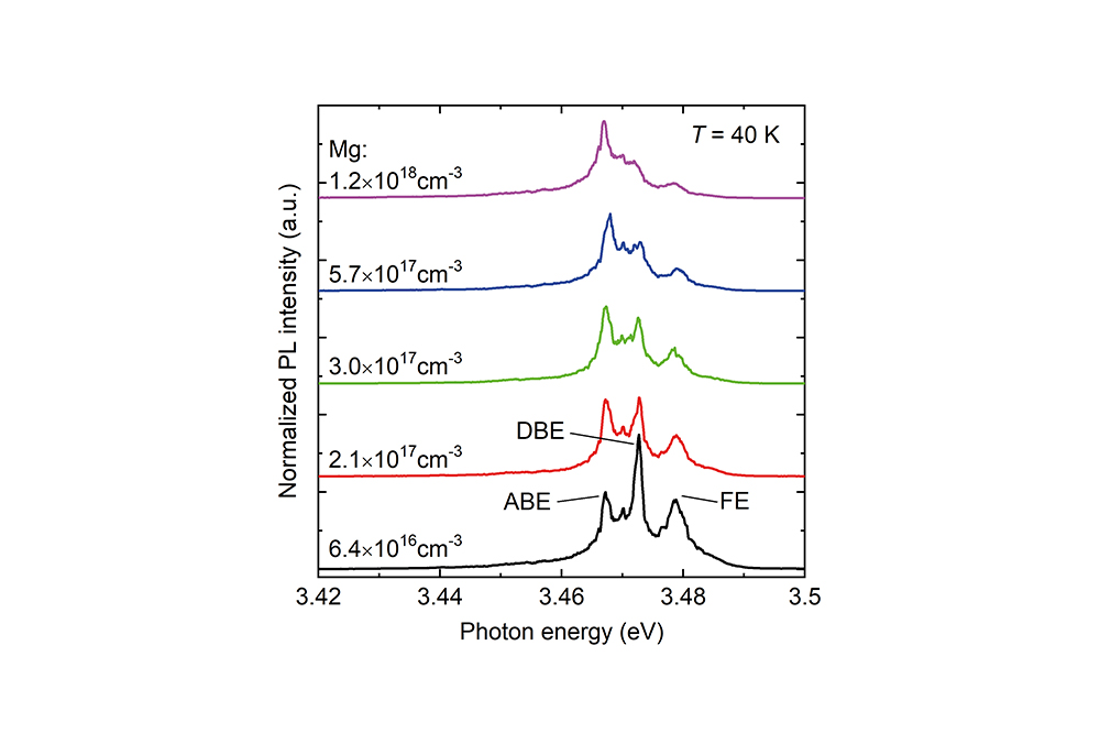
To establish this technique, the team produced five samples, containing 2µm-thick GaN layers with a range of magnesium doping levels from 5 x 1016 cm-3 to 1 x 1018 cm-3. After capping these epilayers with 100 nm of SiO2, they annealed the samples for 5 minutes under nitrogen gas at 1050 degC to activate the dopants. Prior to photoluminescence measurements, the samples were etched to remove the SiO2 cap and the magnesium segregated layer near the surface.
Photoluminescence measurements at 40K produced several peaks, including those associated with the neutral magnesium acceptor-bound exciton (ABE) and the free exciton (FE). See Figure 1 (at the top of this article) which also shows the neutral donor bound exciton (DBE).

Figure 2. Thanks to a power law, magnesium doping levels can be extracted for photoluminescence measurements, by determining the ratio of the intensity of the peak for the neutral magnesium acceptor bound exciton to that of the free exciton
The ratio of the intensity of these two peaks has a power-law dependence with the magnesium concentration, measured by secondary-ion mass spectrometry. See figure 2 above.
The power law established by the team could also be used to determine p-doping levels in LEDs, laser diodes and HEMTs. “However, these devices have high impurity concentrations that are relatively easy to measure electrically, so my technique may not be as beneficial,” says Omori.
According to him, one of the team’s next goals is to create calibration curves for other impurities, such as silicon donors. “Also, since the ion implantation technique has not yet been established for GaN, I am considering applying my technique to its development.”
M. Omori et al. Appl. Phys. Express 14 051002 (2021)


