
Penn State to install Samco surface treatment solutions
US university nanofab to use Aqua Plasma model AQ-2000 and tabletop UV ozone cleaning system for surface modification of substrates that include 2D semiconductors
Samco, a manufacturer of etching, deposition and surface treatment processing equipment, has announced that the Nanofabrication Laboratory at the Pennsylvania State University Materials Research Institute (Penn State MRI Nanofab) has selected a complementary suite of its surface treatment solutions including an Aqua Plasma cleaning system and a UV ozone cleaning system.
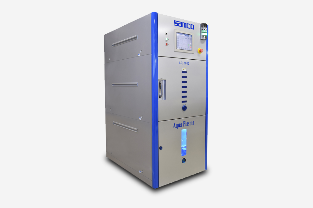
Penn State MRI Nanofab, one of the leading facilities in North America for nanotechnology research/development and prototyping, has selected Samco’s water-based plasma treatment system Aqua Plasma model AQ-2000 and tabletop UV ozone cleaning system, model UV-2 for surface modification of substrates that include 2D semiconductor materials. They operate as an open user facility for nanofabrication with academic, industrial, and government users.
Aqua Plasma is deisgned for efficient and safe reduction of metal oxides, improves bond strength between substrates, enhances hydrophilization, and can be used for ashing or organic removal applications. Not only is this unique surface treatment technique effective, it is also safe to the environment and operators.
Chad Eichfeld, Nanofab director of operations at Penn State’s NF, states: "The flexibility of the AQ-2000 will have long-term impact on the materials research community at Penn State by allowing for the processing of wide range of materials with a more robust and efficient process flow. With the expanding research on devices made with 2-dimensional materials there is a need for plasma etching with both low damage as well as reduced oxidation of surfaces.
"The AQ 2000 is a unique tool that allows for both oxygen and water-based plasma processing that is unique in that it eliminates surface oxidation, a main driver for the system selection. After sending some samples of our 2D materials we found that the water plasma also had the added benefit of reducing the surface damage of the material as well. Another key factor in our decision was the flexibility of having multiple plasma technologies: Down Stream Plasma, Plasma Etching and RIE Etching in the same system. Bundling these capabilities into a single system will allow us to optimize our capabilities while at the same time reducing the equipment footprint in our cleanroom.”
Tsukasa Kawabe, president and COO of Samco, comments: "With our cutting-edge surface treatment technology, Aqua Plasma and UV ozone cleaning, we offer a convincing solution even for world-leading research facility. For more than thirty years, Samco has been delivering plasma processing solutions to universities and R&D facilities in the US. We are truly proud that Penn State Nanofab has now selected our equipment for their open laboratory.”


