
Novel Crystal develops 100mm β-type gallium oxide wafers
β-type gallium oxide power devices can be mass produced
Novel Crystal Technology, Inc has successfully scaled up its high-quality Ga2O3 epitaxial wafer manufacturing technology to 100-mm. It means Ga2O3 power devices can now be produced on a 100-mm mass-production line.
Compared with materials currently in development for use in power devices, such as SiC and GaN), β-Ga2O3 has a larger band-gap energy4 of 4.5 eV5, and it is considered to be an ideal material because it can reduce the loss in power devices.
Moreover, β-Ga2O3 is different from SiC and GaN in that single-crystal substrates can be fabricated with the melt growth method6. High-quality, large single crystals can be grown at 100 times the rate of SiC and GaN, leading to reduced costs. Thanks to these characteristics, the focus is on achieving practical use of β-Ga2O3 power devices in a timely manner.
The company succeeded in fabricating high-quality 2-inch (50.8 mm) Ga2O3 epitaxial wafers in 2019 and has been manufacturing and selling them since the beginning of 2019. However, there is as yet no 2-inch mass-production line for power devices because the manufacturing cost of the devices on 2 inch wafers is too high, and consequently, the use of these wafers has been limited to research and development.
Recently, the firm developed 100-mm β-Ga2O3 epitaxial deposition equipment by applying our high-quality 2-inch epitaxial wafer technology. This advance means that high-quality100-mm β-Ga2O3 epitaxial wafers can now be produced and sold. In particular, β-Ga2O3 power devices can be produced on a 100-mm mass-production line.
In 2015, Novel Crystal Technology, Inc. collaborated with Yoshinao Kumagai and Hisashi Murakami of Tokyo University of Agriculture and Technology and the National Institute of Information and Communications Technology in the development of a β-Ga2O3halide vapour phase epitaxy for β-Ga2O3 epitaxial deposition. By continuing to improve the deposition equipment and process, the technology can be applied to large wafers.
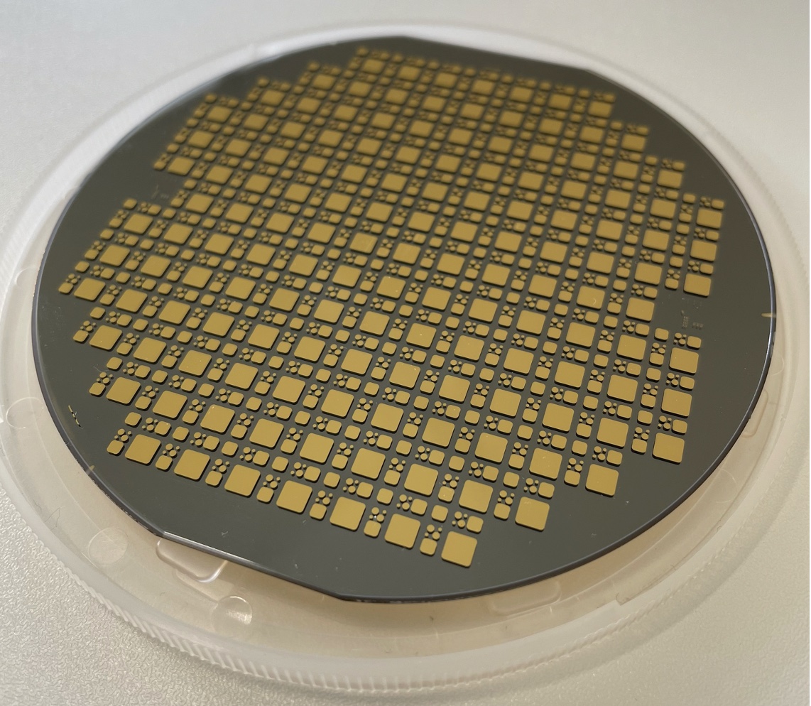
The photograph above shows prototype β-Ga2O3 SBDs fabricated on 100-mm β-Ga2O3 epitaxial wafers.The epitaxial film is about 10-μm thick, and the donor concentration is about 2×1016 cm-3.The yellow circles and squares on the wafer surface are gallium-oxide SBDs with different element sizes.
The graphs below showsthe current-voltage characteristics of the diode. The measurements of 86 elements on the wafer surface are overlaid on each graph. The theoretical characteristics are drawn with a red dotted line in the graph. The forward characteristics in (a) show that the current increases linearly from a low rising voltage of 0.8-0.9 V, and ideal diode characteristics are obtained.

The graph of the reverse characteristics in (b) shows that 62 of the 86 elements show characteristics in line with the theoretical ones, and they can be judged as non-defective products.
The killer defect density8 calculated from this non-defective rate is 13 pieces/cm2. This means that the 100-mm epitaxial wafer has the same quality as a high-quality 2-inch epitaxial wafer. Accordingly, 10-A β-Ga2O3power devices can be produced on a 100-mm wafer with a yield of 80 percent.
Future developments
The company has started selling high-quality100-mm β-Ga2O3 epitaxial wafers. Customers can specify the donor concentration of the epitaxial wafer in a range between 2×1016 cm-3 and 9×1016 cm-3 .
Moreover, the epitaxial film thickness can be specified to between 5 μm and 10 μm. In the future, the firm will work to expand the specifiable ranges of donor concentration and film thickness, further reduce killer defects, and increase the wafer diameter.
Novel Crystal has already succeeded in demonstrating low-loss β-Ga2O3 SBDs with a trench structure. In the future, it will continue to build mass-production technology for trench-type SBDs on a 100-mm line.
Novel Crystal Technology is a venture of Tamura Corporation, that performs the development, manufacture, and sales of β-Ga2O3substrates and epitaxial wafers. It is a technology transfer venture of the National Institute of Information and Communications Technology (NICT), Japan.


