
Gallium oxide vertical transistor has highest breakdown voltage
Breakdown voltage of 4.2 kV is 1.6 times higher than that of conventional transistors
Novel Crystal Technology has developed a β-Ga2O3vertical transistor with the world's highest breakdown voltage of 4.2 kV. This is 1.6 times higher than the breakdown voltage of conventional transistors.
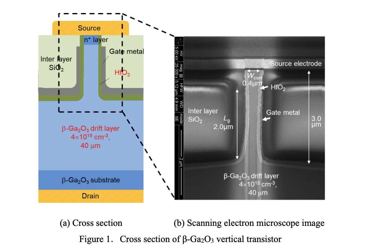
Figure 1 (above) shows a cross section of the newly developed β-Ga2O3 vertical MOS transistor.
The transistor is a vertical device structure that is advantageous for meeting the low-loss and large-current requirements of power devices. A FinFET structure that enables normally off operation without using a p-type conductive layer by narrowing the mesa width to submicron or less. High dielectric constant hafnium oxide (HfO2) insulating film to weaken the electric field strength in the gate insulating film. A high-voltage drift layer with a low donor concentration (4 x1015 cm-3) and thick film (40 μm) formed using our newly developed high-quality thick-film epitaxial growth technology.

Figure 2 shows the drain current-drain voltage characteristics of the fabricated transistor (mesa width 0.4 μm, mesa length 60 μm). The device shows a normally off characteristic in which no current flows at a gate voltage of 0 V, a maximum current density of 2.6 mA/mm, and an on-resistance of 1.2 x 10³ Ω mm. In this transistor prototype, the source n+ layer and the channel layer are separated by about 0.4μm, and it is estimated that the source resistance is high. We believe that it is possible to reduce the on-resistance further by improving the device design.
Figure 3 shows the gate voltage dependence of the drain current and gate current when a drain voltage of 5 V is applied. The drain current on/off ratio is as large as 8 digits or more, the subthreshold coefficient9 is 120 mV/decade, and the gate leakage current is below the measurement limit; good transistor characteristics are thus obtained. On the other hand, the drain current-gate voltage characteristic shows hysteresis of about 0.2 V, meaning that the MOS gate interface needs to be improved.

Figure 4 shows the drain current and gate current characteristics when a positive voltage is applied to the drain electrode with the gate voltage and source voltage fixed at 0 V. Due to the improved controllability of the gate afforded by the FinFET structure and the effect of the high dielectric constant HfO2 insulating film on the bottom surface of the mesa processing, no drain leak current or gate leak current is generated even if a drain voltage up to about 4 kV is applied.
In addition, by adopting a high-quality epitaxial layer with a low donor concentration (4x1015 cm-3) and a thick film of 40 μm as the drift layer, a breakdown voltage of 4.2 kV (1.6 times the previously reported value of 2.6 kV (W. Li et al., IEDM 19-270)) is obtained.
The maximum electric field strength in the β-Ga2O3 drift layer on the bottom surface of the mesa processing is estimated to be 2.5 MV/cm. A two-dimensional device simulation indicated that an electric field concentration several times stronger than this is generated at the gate electrode end. Therefore, the breakdown voltage can be further increased in the future by introducing an electrode termination structure that alleviates the electric field concentration. We believe that low on-resistance can be achieved.
Future development
In addition to solving the problems clarified by studying this device prototype, the research team will work to increase the size and current of the device. Mass production of 600-1200 V medium breakdown voltage devices will begin in 2025 and prepare for mass production of high breakdown voltage devices of 3000 V or higher.
The low cost of β-Ga2O3 semiconductors for use in the medium breakdown voltage region is an advantage for electric vehicles and other commercial applications. We will proceed with development to reach our goal.


