
Getting complex semiconductors to self-assemble
New method grows 2D perovskites precisely layered with other 2D materials to produce crystals with a wide range of electronic properties.
Stacking extremely thin films of material on top of each other can create new materials with exciting new properties. But the most successful processes for building those stacks can be tedious and imperfect, and not well suited for large-scale production.
Now a team led by Stanford Professor Hemamala Karunadasa has created a much simpler and faster way to do it. They grew 2D layers of one of the most sought-after materials, known as perovskites, interleaved with thin layers of other materials in large crystals that assemble themselves.
The assembly takes place in vials where the chemical ingredients for the layers tumble around in water, along with barbell-shaped molecules that direct the action. Each end of a barbell carries a template for growing one type of layer. As the layers crystallise – a process similar to making rock candy -- the barbells automatically link them together in the proper order.

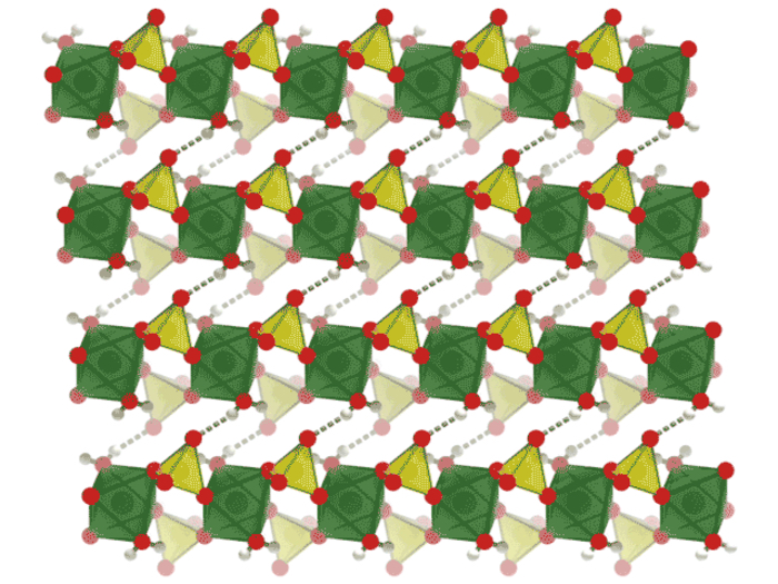
The diagram above shows how the layers of two 2D materials – a perovskite (blue) and a metal halide (yellow) – assemble themselves out of chemicals tumbling around in water (left).
“What’s really cool is that these complex layered materials spontaneously crystallize,” said Michael Aubrey, who was a postdoctoral researcher in Karunadasa’s lab at the time of the study.
The researchers say their method lays the foundation for making a wide array of complex semiconductors in a much more deliberate way, including combinations of materials that have not been known to pair up in crystals before. They described the work in a paper published in Nature today.
“We are pretty thrilled about this general strategy that can be expanded to so many kinds of materials,” said Karunadasa, who is an investigator with the Stanford Institute for Materials and Energy Sciences (SIMES) at the Department of Energy’s SLAC National Accelerator Laboratory.
“Rather than manipulating materials one layer at time,” she said, “we’re just throwing the ions into a pot of water and letting the ions assemble the way they want to assemble. We can make grams of this stuff, and we know where the atoms are in the crystals. This level of precision allows me to know what the interfaces between the layers really look like, which is important for determining the material’s electronic structure – how its electrons behave”
Easy to make, hard to stack
Halide perovskites – materials that have the same octahedral structure as naturally occurring perovskite minerals - have been assembled in water since the 1900s, Aubrey said. They have a lot of potential for efficiently absorbing sunlight in solar cells and converting it to electricity, but they’re also notoriously unstable, especially in the hot, brilliantly lit environments that photovoltaics operate in.
Layering perovskites with other materials could combine their properties in ways that improve their performance in specific applications. But an even more exciting prospect is that entirely new and unexpected properties could emerge at the interfaces where layers meet; for instance, scientists have previously discovered that stacking thin films of two different types of insulators can create an electrical conductor.
It’s hard to predict which combinations of materials will turn out to be interesting and useful. What’s more, making thinly layered materials has been a slow, painstaking process. Layers are generally made by peeling films just one or two atoms thick, one at a time, from a bigger chunk of material. That’s how graphene is made from graphite, a pure form of carbon used in pencil leads. In other cases, these thinly layered materials are made in tiny batches at very high temperatures.
“The way they’re made has not been scalable and sometimes even difficult to reproduce from one batch to another,” Karunadasa said. “Peeling off layers that are just one or two atoms thick is specialized work; it is not something you and I can just go into the lab and do. These sheets are like a very flexible deck of cards; when you take one out, it can crumple or buckle. So it is hard to know the exact structure of the final stack. There is very little precedent for materials that look like the ones we created in this study.”
Rock candy synthesis
This work grew out of research by study co-author Abraham Saldivar Valdes, a graduate student in Karunadasa’s group at the time. Over the course of several years, he developed the new method for getting the layered structures to assemble themselves, which was further expanded by graduate student Bridget Connor. Meanwhile, Aubrey discovered that their atomically thin layers had the same structure as 3D blocks of similar materials whose properties were already known, and he tracked how the two different layers have to slightly distort to share an interface. He also studied the optical properties of the final products with the help of graduate student Kurt Lindquist.
Creating the layered structures “is the same exact process as making rock candy, where you drop a wooden dowel into saturated sugar solution and the candy crystals seed themselves onto the dowel,” Aubrey said. “But in this case the starting materials are different and you don’t need a dowel – crystals will start forming in water or on the surface of the glass vial.”
The team made six of the self-assembled materials, interleaving perovskites with metal halides or metal sulfides, and examined them with X-rays at the Advanced Light Source at DOE’s Lawrence Berkeley National Laboratory.
In most of the structures, the barbell molecules held the layers slightly apart. But in one of them the barbell molecules brought the layers directly into contact with each other so they could form chemical bonds.
“We are particularly excited about this type of structure where the layers are connected because it could lead to emergent properties, like electronic excitations that are distributed across both layers,” Karunadasa said.
“And in this particular case, when we hit the material with light to free electrons and create positively charged holes, we found the electrons mostly in one type of layer and the holes mostly in the other. This is important in our field, because it allows you to tune those two environments to get the electronic behavior you want.”
With the new technique in hand, Aubrey said, “We’re doing a lot of exploration now to discover what kinds of structures can be made with it.”
Marina Filip and Jeffrey Neaton from the University of California, Berkeley and Berkeley Lab performed the electronic structure calculations in this work. This research was funded by the DOE Office of Science. ALS is an Office of Science user facility, as are two other facilities where computing was done for this research: the National Energy Research Scientific Computing Center (NERSC) and the Oak Ridge Leadership Computing Facility.
Ref Michael Aubrey et al., Nature, 15 September 2021 (10.1038/s41586-021-03810-x)


