
Feel-good factor flowed through CS International 2021
Delegates were delighted to attend an in-person conference championing the tremendous opportunities for compound semiconductors in communications, displays and automobiles
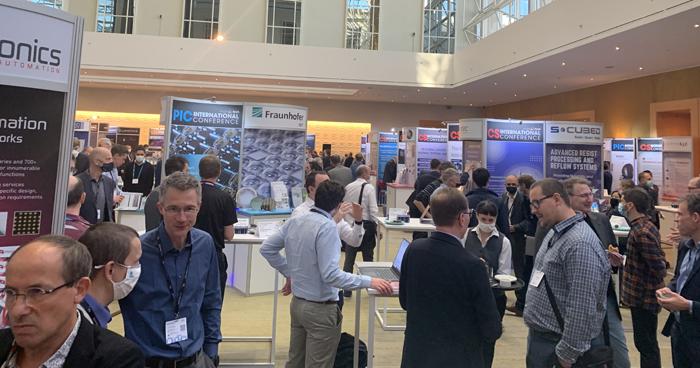
The many delegates attending this year’s Compound Semiconductor (CS) International, held at the Sheraton Hotel at Brussels Airport on the 9th and 10th on November 2021, delighted in the in-person format.
Attendee numbers were incredibly healthy (despite Covid-19 hampering travel from China, Japan and South Korea )with many enjoying face-to-face meetings within the compound semiconductor community for the first time since the start of the pandemic.
Those at the conference were able to hear 30 talks, divided into five key themes: satisfying demand for more data; seeking new opportunities for LEDs and lasers; taking wide bandgap devices to their ultimate limits; ramping volumes in the power electronic sector; and enhancing the automobile.
Delegates could also drop in on presentations at Photonic Integrated Circuits (PIC) International and Sensors Solutions International (SSI), and talk to company representatives at an exhibition housing over 70 exhibitors.
As well as the feel-good factor that came from attending this vibrant event, delegates at CS International were buoyed by the positive outlook for this industry. According to a handful of presentations provided by analysts from Yole Développement, all the key sectors within this industry are set to enjoy growth over the coming years.
Helping to fuel this are many opportunities for sales of GaAs-based and GaN-based transistors for communication infrastructure, argued Claire Troadec, Power & Wireless Division Director at Yole. Troadec pointed out that GaAs devices are viable contenders for the switch, the low-noise amplifier and the gain block (PA). She added that in the final-stage PA, the battle is raging between LDMOS and GaN, but GaN will emerge as the winner in the longer-term. Looking ahead, she expects GaAs to prevail in backhaul, while GaN will enjoy success in sub-6 GHz 5G. This will help to swell annual sales for GaN RF devices, which are tipped to climb from almost $1 billion today to nearly $2.5 billion by 2026.
Troadec also offered some insight into the smartphone market, where GaAs dominates amplification. She described the RF front-end as the biggest opportunity for RF components, with the wide bandwidth for amplification requiring the use of several PAs. The introduction of 5G has increased GaAs content in the phone, with the latest communication standard leading to more than 4 mm2 of GaAs in an entry level phone, and more than 6 mm2 in a luxury variant.
Increased penetration of 5G smartphones is leading to growth in the volume of substrates consumed for the production of GaAs RF devices. Calculated in terms of 150 mm wafers, there are now around 600,000 wafer-starts per year, a figure that is on a slight rise. Troadec is predicting GaN-on-silicon to make a small but growing impact on this sector.
Within the power electronics sector silicon still dominates, but wide-bandgap devices are tipped for a rapid growth in sales over the coming years. SiC devices are forecast to generate the greatest revenue, spurred on in part by the expansion in production capacity at the likes of Wolfspeed and STMicroelectronics. However, sales for GaN should also grow at a healthy rate, as this class of device expands from serving in fast chargers for smartphones to deployment in other applications, including automobiles.
Championing the capabilities of GaN, Philip Zuk, Senior Vice-President of Technical Marketing and Business Development at Transphorm, made a strong case for the use of this device at various voltages, including some considered to be the domain of SiC.
Transphorm is a world leader in GaN power devices: it employs more than 100 staff, it has more than 1,000 patents, and it has generated revenues of nearly £13 million in 2021. This vertically integrated chipmaker produces its epiwafers on five 6-inch MOCVD reactors, with material processed in a high-volume wafer fab in Japan through a joint venture. Defect densities in its material are no higher than those found in silicon CMOS epiwafers, and devices have been qualified according to several standards, often breaking new ground.
During Zuk’s talk, he compared the performance of a SiC FET, SiC MOSFET and Transform’s SuperGaN. When evaluating these three, in turn, in a 12 kW application, the SuperGaN is found to run more efficient and cooler than both forms of SiC. Adopting an upper limit on the device temperature of 165 C, the maximum power when using the SiC FET and SiC MOSFET is restricted to 9.2 kW and 11 kW, respectively. With the GaN FET, the junction temperature is just 139 C at maximum power, leading to a power loss of only 102 W. In comparison, the use of SiC FETs and SiC MOSFET incurred losses of 164 W and 130 W, respectively.
Another exciting opportunity for compound semiconductor devices is in the display industry, where microLEDs could be used to provide direct emission, leading to higher efficiencies and contrast ratios. Samsung showcased the first commercial luxury MicroLED TV earlier this year, but prices must tumble if this technology is to be used for mass deployment.
Yole’s Business Unit Manager for Solid-State Lighting and Display, Pars Mukish, offered some options for doing this, telling delegates that the biggest opportunity for slashing costs is to shrink the size of the LED. Mukish estimated cost reductions ranging from a factor of 4 to 70 by diminishing die size. According to him, a very significant impact could also come from improving yield and repair, and from streamlining transfer and assembly: these two options could lead to cost reductions of up to 50 times and 120 times, respectively. Further gains could come from an increase in manufacturing efficiency, which could halve costs.
If fabs are to make tiny microLEDs in high volumes with a high yield, they will need to invest in new equipment. Many companies are offering tools that will help in this endeavour. At CS International, Veeco described how its latest single- and multi-wafer tools can provide more uniform epiwafers; Attolight outlined how cathodoluminescence can scrutinise wafers for their optoelectronic characteristics; and Evatec and Beneq detailed approaches for forming distributed Bragg reflectors that can boost optical output in vertical LEDs.
Given the strong demand for face-to-face interaction, delegates will be pleased to note that they will not have to wait a whole year for the next CS International. The next instalment, which will be the 11th CS International, will be held in June 2022 at the Sheraton Hotel, Brussels Airport.


