

Hybrid bonding: Going for GOLD
Hybrid bonding provides attainable scaling for packaging of compound semiconductor devices in copper or gold
BY JOHN GHEKIERE FROM CLASSONE TECHNOLOGY
Fabricating semiconductor devices begins by growing epiwafers, with efforts directed at ensuring high-quality crystalline material with minimal imperfections. Once a device is completed, it often has to be integrated into its CMOS brain in order to carry out its impressive tasks. Commonly this integration is accomplished by employing advanced packaging techniques, many of which include some form of pillar formation and bonding. However, continued input/output (I/O) scaling is taking conventional packaging approaches and putting them out of reach for many manufacturers. Hybrid bonding offers abundant opportunity for I/O density scaling.
Increasing in popularity, heterogeneous direct bonding, also known as hybrid bonding, is a technology that involves directly bonding dielectric and interconnect features, either between two wafers, or between a chip and wafer. Such a concept is not new, having been studied and developed over the course of more than a decade, and already deployed in the manufacture of some CMOS image sensor devices. Yet, until recently hybrid bonding has not gained widespread traction as a viable approach for packaging integration. But that is changing.
The exponentially increasing technical difficulties associated with the scaling more well-established approaches, primarily based on pillars, has driven interest in hybrid bonding, along with a hike in its funding. The challenges of scaling that are facing leading-edge pillar applications are so great that they are putting enabling input/output density scaling out of the reach for most device manufacturers.
This limitation is a major blow for compound semiconductor device manufacturers operating in this highly competitive marketplace. As the majority of dollars spent on development are largely committed to true device technology, there is little funding left to try and advance an already profoundly advanced packaging flow. Adding to the woes of the compound semiconductor industry are the relatively small R&D budgets compared with those of the manufacturers of silicon-based devices. Foundries are an option, but as compound semiconductor devices are still largely produced on wafers with a diameter of 150 mm or less, finding a foundry operating at these wafer diameters and yet capable of such advanced packaging integration is becoming impossible.
Fortunately, hybrid bonding offers a genuine alternative. This approach is clearly important, justifying expenditure on development that should offer a great return. While some investment optimisation is valuable, there is the promises of multiple generations of incremental innovation, an attractive proposition compared with the diminishing returns that characterise further pillar development.
For pillar and bump packaging, a 10 mm by 10 mm ‘micro-pillar’ represents the state of the art. To scale the pitch any further is challenging to even the most advanced manufacturers in the industry. Progress on this front would allow an increase in the number of inputs and outputs on a device – realising this requires increasing the feature density, and in turn decreasing the pitch and ultimately making the feature narrower. As the pillar is a truly three-dimensional structure, if there is no scaling of its height, this leads to a mechanical integrity problem. To prevent this from arising, engineers must scale for height, meaning that maintaining an incredibly tight variation feature-to-feature actually produces an exponentially greater percent difference, known as coplanarity. Uniformity cannot stay the same or even incrementally improve. It must improve greatly, feature to feature. The unwanted consequences are genuine challenges in realising the coplanarity necessary to yield.

Direct bonding of gold pads for emerging devices
Can such coplanarity be achieved? At present, yes, and great achievements are continuing in this regard. But each new scaling requires development of new plating chemistries and equipment modifications, alongside a level of novelty in innovation that tends to result in new patents and exclusive IP. All of which means more cost. Can it be done? Yes – and it is being done. However, given the growing difficulties, progress that is demanded is inaccessible to all but a few manufacturers.
There are also challenges to conventional packaging that go beyond plating and mechanical integrity. Consider lithography. The photoresists used in pillar/bump packaging integration are just one of the many marvels produced in the semiconductor industry. They have to be compatible with a multitude of plating electrolytes with values for pH ranging from just 1 or 2 to as high as 9 or 10; a genuine compatibility challenge for resist formulation. There is a trade-off when using a highly robust resist material. It creates challenges for removal, solved using processing steps that are chemically and mechanically aggressive. Again, does it work? Yes, so far. However, it serves to further narrow an already narrow process window that arises because the plated features, composed of multiple metals (think adhesion), are incredibly small, free-standing structures. There are also practical considerations associated with the sheer precision of the feature dimensions of a photoresist operating at these sizes. Progress is being made, but these advances are coming from fewer and fewer manufacturers.
Hybrid heaven
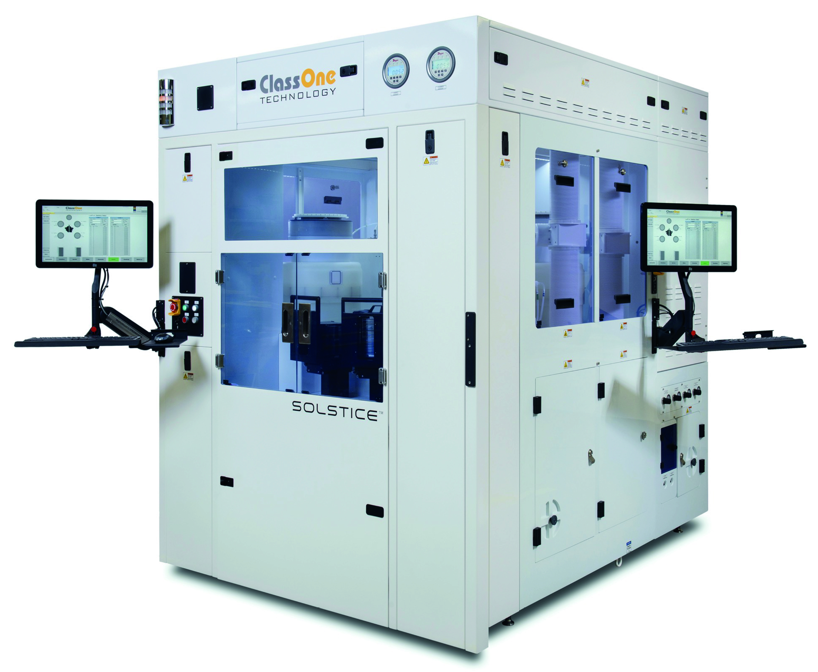
Switching from the use of pillars to hybrid bonding greatly simplifies many of the issues that are associated with plating, mechanical integrity and lithography. For starters, hybrid bonding employs plating capabilities that have already been established for far smaller feature sizes and a narrower pitch. Take copper metallization, the most common implementation of hybrid bonding: CMOS interconnects have already driven the development of feature fill plating to dimensions below 100 nm, which is more than three orders of magnitude smaller than that associated with pillars. What’s more, this drove the filling of much higher aspect ratio features than those required for hybrid bond applications. When focusing on plating, we can see that the advances necessary for four, five or even six additional generations are already largely established and feasible. The CopperMax reactor from ClassOne Technology represents an advanced plating cell designed to deliver such extensibility in copper fill for hybrid bonding applications.

Novafab nano-twin copper, optimal for direct bonding
Another merit of hybrid bonding is that it employs no free-standing structures. By instead relying on embedded pads of metal, this technology supports a level of scaling that, in terms of plating capability, is already well established beyond the current constraints in wafer alignment. So advanced is this scaling that it is driving advances in wafer alignment.
To illustrate this point, let’s consider copper plating. For many of today’s manufacturers of devices designed around the pillar/bump process, the extremely advanced 20 mm pitch is unattainable. But this length scale is easy to realise with copper damascene plating. This form of plating has been used for advanced logic interconnects. Although copper plating has recently been displaced by PVD reflow, and in some cases cobalt, at the most advanced nodes, copper plating was the process of record through to the 10 nm node where metal 1 via dimensions reached the scale of around 30 nm or less.
For hybrid bonding, the feature scale associated with the current state of the art is an input-and-output density of around 10 mm and even lower. Thanks to success at this length scale, wafer-to-wafer bonding is available not only as a general die stacking or packaging scheme for large manufacturers that are likely to be slower to adopt it, but also to the many smaller innovators of devices as such microLEDs, advanced RF devices, and other discretes. The technology can be employed for both wafer-to-wafer bonding and for pick-and-place.
When evaluating different options for unit materials, it is essential to consider not only the plating step, but the processes that surround it – and thus consider the pros and cons compared with those associated with pillar integration. Embedded pad plating, often known as feature fill, does require an advanced chemical mechanical polishing (CMP), which precisely planarizes metal and dielectric. Existing copper CMP routinely planarizes feature densities to a level several orders of magnitude higher than that needed for today’s state of the art packaging.


Sub-micron feature filled with gold. Void-free. The aspect ratio is 1.5:1. Top Right: A magnified image, showing two sub-micron features filled with gold
This is not to say that advanced copper CMP is simple, but rather that the necessary development was already driven by advanced interconnect integration and thus already exists. Specific to direct hybrid bonding, the CMP must accommodate the difference in the coefficient of thermal expansion between the dielectric and metal. Complete and reliable bonding demands that the metal bond pads be slightly recessed but precisely so, typically to within 5 nm of specified recess. Thus after the bonding step that unifies the dielectric, the ensuing bonding step for the metal results in an expansion of the two interfacing pads which grow into each other and ultimately form a monolithic interconnect. Again, not trivial, but not a new requirement either.
Copper versus gold
For hybrid bonding, the post-CMP cleaning becomes truly critical. When using copper, there is an established process of record for engineers to draw on. Cleaning chemistries for device metallization have been established that realise excellent particle removal, low residual surface contamination of metal ions and effectively zero metal etching on the exposed features. This is a unit process step that is already established though requires very tight process control.
Interestingly, and perhaps to some surprisingly, metallization in gold offers a realistic alternative to copper. Though clearly not as advanced overall, a great deal of development has been directed at metallisation with gold, including the establishment of a highly competitive pilot production line for emerging device types. Within this line, the GoldPro reactor developed by our team at ClassOne Technology of Kalispell, Montana, provides a plating Process or Record. Many manufacturers are yet to consider gold in damascene-like, or recessed, plating architectures, despite much effort at developing this technology, which has included establishing pilot production. Compared to copper, gold has also received far less attention for the additive development for superconformal fill, but it has proven to be significantly less susceptible to seam voids. While much more expensive than copper, gold has many key virtues, including resistance to corrosion. In some applications, these strengths warrant the use of this precious metal.
Our team has shown that by combining proper chemistry formulation with key parameter controls, in our specific case MadDermid Enthone’s MicroFab Au660 sulfite gold electrolyte and our GoldPro reactor, employing specific plating waveform and electrolyte flow profile, an effective and scalable feature fill with gold is readily available today. Working with a key manufacturing partner in an emerging technology, we have developed and demonstrated a gold feature fill of a pad feature with a 1.5:1 aspect ratio. This is a far tighter pitch than that for a pillar/bump involving a 10 mm-wide copper pillar, which is considered to be state of the art for that technology.
The development of gold CMP technology is not as mature as copper CMP, and is subject to a similarly tight process window with regard to metal recess. Of particular challenge is the fact that gold CMP chemistries tend to be considerably more aggressive than those for copper. If aggressive slurries are employed, there are challenges to face in forming a sufficiently smooth dielectric surface while
controlling the recess of the gold features. As with copper, a hybrid bond sequence begins by direct bonding the dielectric surface, followed by bonding of the metal.
When it comes to optimizing the grain structure for the most efficient bonding, copper metallization has again received more attention than gold. That said, gold has already been shown to be platable in distinctly different orientations, suggesting that there is ample room for near-term optimization.

Gold plated in multiple crystal orientation using MicroFab Au660 gold sulphite chemistry, supporting optimization for direct bonding
At some point even gold’s forgiveness to conformal plating and its avoidance of seam lines will give way to the realities of a higher aspect ratio for which conventional gold electrolytes will not suffice. However, since the feature is equivalent to a pad, its current-carrying capacity is defined in the horizontal, not vertical. In other words, the bond pad does not need to be tall to work, so it is unlikely that there will ever be a need to produce a pad with a feature of an excessive aspect ratio. Development may drive towards a ratio of 2:1, with deployment requiring a fill step that more directly resembles true bottom-up plating. Such efforts are already well underway, with significant progress achieved by MacDermid Alpha.
One practical constraint to further development of a more bottom-up gold chemistry technology is the ability to accurately analyse such chemistry. The difficulty stems from being unable to draw on all the conventional electrochemical analysis methods. For copper plating chemistries, which depend on forward and reverse plating – that is, plating and stripping – a rotating disc electrode is used. Gold cannot be readily stripped in a similar way. Fortunately, these challenges could soon disappear, as progress is being made, including novel development by Ancosys GmbH.
Many may wonder why it makes any sense to use gold, rather than copper, given the far higher costs – gold currently commands around $1800 an ounce, compared with just $5 for copper. There are, in fact, two reasons for this move: one is technical, while the other based on the market. Ultimately, chosing gold over copper will impose some trade-offs. Gold CMP, as mentioned, will provide tougher challenges than copper CMP. However, gold potentially opens the process window for steps such as the highly critical post-CMP clean step.
With gold, as with copper, post-CMP cleaning is critical to successful hybrid bonding. With copper, there is the threat of oxidation and the criticality of queue times between steps. It is possible to avoid this and realise a high yield – this is the case in the manufacture of CMOS image sensors – but as scaling continues, requirements around precision recess of the pads are to become more stringent, and there will be an increase in sensitivity to small variation. With gold, as there are no oxidation issues, there is a far wider choice of chemistries for post-CMP cleaning as well as intra-step queue times. Additionally, there is far less concern over: the presence of dissolved oxygen in the chemistry; the exposure to air in a moist environment; and other, related complications.
It is also worth noting that that most compound semiconductor do not move wafers through the fab with overhead transport in a hermetically sealed container. This implication is that there is the threat of environmental variation, which is incredibly costly to address. With gold, the chances are that this is far less of an issue. While you may have to work on your CMP step, you don’t have to rebuild your fab!
From a market perspective, there is obviously a higher cost associated with adding a single layer of gold on the surface. However, the contribution to overall production costs is relatively small. And weighing against this additional expenditure is the wider process window that promises to speed integration with a high yield, crucial to unlocking the door to capturing market share. This can make all the difference between enjoying success in an emerging market and missing out on an opportunity.
Within the semiconductor industry, as technologies advance, they often go out of reach of all but the largest manufacturers. When this happens, new approaches emerge that enable continued innovation, leading to countless technological marvels that enthral consumers. This unfolding of events is behind the development and uptake of hybrid bonding. Whether using conventional copper metallization or gold metallization, this is a process that fabs can adopt, thanks to the availability of commercial tools, such as those we have produced.
The author would like to thank Dr Robert Rhoades, recognized CMP expert, for his contributions to this article.


