
Two-photon spectroscopy exposes defects in multi-junction cells
Imaging by two-photon excitation provides a non-destructive method for identifying threading dislocations within inverted metamorphic solar cells
A Japanese collaboration has shown that two-photon excitation spectroscopy is a powerful technique for exposing threading dislocations in the graded buffer layers of inverted metamorphic solar cells.
In inverted metamorphic solar cells, including the record-breaking six-junction cell produced by NREL that has an efficiency of 47.1 percent, threading dislocations form during the strain relaxation of heteroepitaxially grown layers, potentially degrading the device’s electrical characteristics.
Options for minimising the creation of these damaging dislocations are to use of a slightly mis-cut substrate and to introduce an InGaP superlattice – both control misfit dislocation glide-planes in the buffer layers. However, controlling these glide planes is not easy, leading to variations in the efficiency of solar cells produced from a single wafer.
Reducing the threading dislocation density across these epiwafers would increase efficiencies. According to a study reported back in 1985, there is a practical upper limit for the threading dislocation density in this material system of 105 cm-2.
Two established techniques for evaluating the threading dislocation density in graded buffers are electron-beam-induced current and cathodoluminescence measurements. However, both lead to simultaneous excitation of several buffer layers, hampering efforts to pinpoint the location of the threading dislocations.
Addressing this weakness is the two-photon excitation spectroscopy approach employed by the Japanese team, which is a partnership between researchers at the Japan Aerospace Exploration Agency, Osaka University, Sharp Corporation, and the National Institute of Advanced Industrial Science and Technology.
The optical technique they employ has previously been used by another team to expose threading dislocations in bulk GaN. In that work, researchers constructed a three-dimensional map of the dislocations by scanning the focus of the excitation light through the sample.
It is challenging to apply this approach to inverted metamorphic multi-junction solar cells, because the high refractive indices of the materials elongates the focal spot in the depth direction. However, by selecting an appropriate detection wavelength, corresponding to the bandgap of the layer under investigation, it is possible to image thin layers.
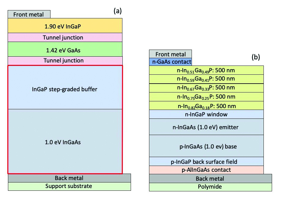
The Japanese collaboration has used a Nikon A1MP two-photon excitation microscopy system to investigate three samples: a triple-junction inverted metamorphic cell based on InGaP, GaAs and InGaAs; and a pair of single-junction InGaAs cells with different open-circuit voltages. The figure above shows how two-photon excitation spectroscopy can identify threading dislocations in the graded buffer layers of inverted triple-junction (a) and single-junction (b) metamorphic solar cells. The combination of the step-graded buffer and InGaAs junction in the single-junction cell is similar to the structure surrounded by the red rectangle.
Employing detection above 750 nm enabled determination of the density of nonradiative recombination centres in the buffer layer next to the active layer of the single-junction cells. The team recorded a density of dark spots of 7 x 106 cm-2 in the sample with the lower open-circuit voltage, compared with 3.3 x 106 cm-2 in the better-performing device.
Turning to X-ray diffraction, the researchers found that the distribution of preferential glide planes has a higher degree of homogeneity in the sample with a higher open-circuit voltage. This result highlights the strength that comes from combining two-photon excitation microscopy with X-ray diffraction.
REFERENCE
† A. Ogura et al. Appl. Phys. Express 14 111002 (2021)


