

Towards efficient spaceborne millimetre-wave transmitters
Through the project Kassiopeia, a European team is developing
highly-efficient microwave and millimetre-wave amplifiers based on
an iridium-sputter gate technology and a novel buffer
BY JOACHIM WÜRFL FROM THE FERDINAND-BRAUN-INSTITUT, BERLIN
OVER THE LAST DECADE and more, there has been a significant increase in the maturity of GaN transistors and MMICs for microwave applications. Improvements in this regard, reflected in the technology readiness level, are allowing engineers to now implement these devices into mission critical systems.
One example of this is the deployment of decentralised microwave power sources in space applications. In this case, using GaN opens the door to light-weight, electronically controlled beam-steering systems, powered with many pixels of active antennas.
Designers of such systems need to consider the pros and cons of using GaN, which majors on flexibility and low weight, but is compromised by its efficiency. To address this shortcoming, it is incredibly important to bundle existing technologies and optimize them along the whole value-added chain – from the semiconductor substrate to epitaxy, processing, circuit design and system implementation.
Our team is taking this approach through a project that commenced on 1 March 2021 entitled Kassiopeia – an acronym for Ka-band MMICs using novel epitaxy, processing and circuit concepts towards highly efficient GaN and AlN devices. We are supported by the European Space Agency, in the frame of the ARTES Advanced Technology initiative on European Ka-band high-power solid-state technology for active antennas. To meet our project’s goals, we are drawing on the expertise of several European partners. It is only through collaboration and the ensuing optimization of devices that incorporate many different technologies that we are able to develop highly-efficient microwave and millimetre-wave amplifiers. Together we are aiming to address self-heating, as well as static and dynamic loss mechanisms, as they are known to adversely influence power amplifier efficiency.

Figure 1. Through the Kassiopeia project, a European collaboration is pursuing holistic technology improvements that aim to enable high power, efficient Ka-band transistors and amplifiers.
Varying roles
A key partner in our project is the epitaxial wafer provider SweGaN. This company is renowned for its fabrication of GaN epitaxial stacks for millimetre-wave transistors. These stacks feature a significantly reduced thermal impedance between the heat source in the device and the heat sink, together with minimized dispersive dynamic effects due to the proprietary epitaxial structure. It is a virtue that comes from the proprietary buffer-free epitaxial approach, which ensures an efficient heat drain to the semi-insulating SiC substrate.
Also playing an important role in Kassiopeia is the Ferdinand-Braun-Institut (FBH). When it comes to GaN RF devices, its unique selling point is its iridium sputter-gate technology, which reduces dynamic losses – that is, gate lagging – to typically just 5 percent. This value is at least half of that of competing institutional and industrial technologies. Additional attributes include a high level of reliability, which is especially important for spaceborne devices. What’s more, FBH has a proven track record in GaN MMIC design, processing and circuit characterization, undertaken in one of the best equipped labs in Europe.
Another key player in the Kassiopeia project is the team at the University of Bristol. They have extensive experience of thermal simulations, combined with direct measurements of the heat source temperature distribution in active GaN FETs. The over-arching goal of Kassiopeia is to holistically improve Ka-band MMIC efficiency, power density, linearity and reliability. Success will come through a systematic analysis of current technology, with respect to parameters that increase device efficiency, linearity and millimetre-wave power density.
Chasing targets
Several parasitic elements are still limiting the performance of GaN-based MMICs (see Figure 1 for an overview of the most important parasitic elements). Through Kassiopeia, we will be developing and refining innovative technological concepts to reduce parasitic elements and incorporate them with novel MMIC design concepts. Our target is to demonstrate GaN MMICs, operating in the frequency band spanning 17.3 GHz to 20.2 GHz, at a power level of up to 43 dBm, while delivering a power-added efficiency of 50 percent and a noise-power ratio of 15 dB.
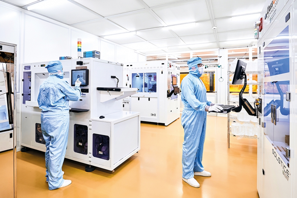
Our development is supported by innovative processing equipment and characterization tools, available at FBH thanks to funding within the framework of the Research Fab Microelectronics Germany – FMD. When making these developments, much consideration is given to the possible transfer of our technology to one of Europe’s GaN foundries.

Figure 2. FBH baseline technology for X and Ka-band MMICs: (left) 150 nm gate using iridium-sputter technology to fully conformally coat the gate trench; (right) an air-bridged X-band power cell using source-connected field plates.
Substantial technological efforts are being made within Kassiopeia to trim parasitic resistances and increase thermal coupling between the heat source, located in the device’s channel region, and the SiC substrate. All optimisation involves FBH’s 4-inch GaN Ka-band process line, featuring iridium-sputter gate technology (see Figure 2).
When developing high-performance microwave power amplifiers, it is crucial to reduce the transistor knee-voltage, because this ensures efficient use of the load-line offered by the device. With highly scaled millimetre-wave devices, total on-resistance may be dominated by the transfer resistance of the source and drain ohmic contacts. To minimise this, there is a need to drive down the ohmic contact resistance, the sheet resistance between source and drain, and the total sheet resistance (see Figure 1).
Factors that influence the contact resistance include the metallurgy of the contacts, as well as the quality, doping and bandgap energy of the semiconducting material underneath it. To try and trim the contact resistance, we are investigating the impact of increasing the AlGaN barrier doping by local ion-implantation. After implantation, we deposit and activate a refractory ohmic contact, which has the hallmark of an extremely precise edge acuity. Thanks to this attribute, we drive down the contribution of the channel sheet resistance to the total source resistance, and thus deliver a further reduction in the knee voltage.
Improvement is also been pursued in the metallic gate strip. Efforts are being directed at increasing its electrical conductivity, because this will enable a more flexible and efficient design of millmetre-wave power cells. Success could come from introducing longer gate fingers per cell – this trims taper losses for more extended power cells. To explore this possibility, we are developing a high-aspect-ratio gate metallization with a comparably low contribution of parasitic capacitances. Key to this is innovative electroplating techniques, utilising FBH’s sputtered iridium gate process to temporarily provide a plating base.
Ensuring efficient power amplification and reliable device operation hinges on a reduction in the thermal impedance between the transistor’s heat source and the SiC substrate. To optimise heat transfer from the device to the substrate, we employ SweGaN’s QuanFINE buffer technology. This platform enables direct growth of a high crystalline quality epitaxial stack, featuring a GaN channel on top of a thin AlN nucleation layer (see Figure 3 for a comparison between this approach and the conventional method). Merits of the use of the QuanFINE buffer technology extend beyond very good thermal coupling. The AlN back-barrier efficiently confines electrons to the channel, thereby enhancing the breakdown voltage for a given gate-drain distance. The upshot, as we’ll soon see, is higher power-density transistor designs.

Figure 3. Comparison of standard epitaxial approaches for GaN microwave transistors and the QuanFINE concept proposed by SweGaN.
Putting it all together
We will use all the technologies discussed to enable innovative power-cell designs. This will enable us to integrate larger gate peripheries into one transistor cell, and in turn increase the respective power level and power density. Ultimately, this will lead to a higher total amplifier power, alongside greater linearity and bandwidth.

Figure 4. Scanning the internal heat source of transistors by micro-Raman technology. The technique can be applied from the top of the device, and also from the underside, through an opened backside metallization.
One downside of a higher power density is that it exacerbates confined heat generation. Consequently, it is indispensable to undertake thermal considerations. In the Kassiopeia project we are doing this, with those at Bristol University taking the lead and offering much insight into the thermal designs of power cells. Efforts involve thermal simulations, and correlation of these results with thermal characterizations using micro-Raman techniques that provide a sub-micron spatial resolution (see Figure 4).
The team at Bristol uses a focused laser beam to scan the device, either from the top, or from the bottom through window openings in the backside metal. The latter orientation enables thermal device characterization of field-plated devices. Whichever geometry is employed for this measurement, micro-Raman characterization provides a precise mapping of the transistor’s heat source. This enables the thermal fingerprint of any modification in device technology and layout to be directly revealed. By adopting this approach, the thermal modelling base is iteratively improved, ultimately leading to well-engineered Ka-band power cells.
To optimize targeted-power MMICs at the circuit level, our collaboration is focusing on low-loss combining, alongside the implementation of highly efficient, harmonically tuned amplifier concepts such as class-F, class-F-1, and Class-J. These concepts provide proper termination of harmonics and significantly reduce transistor losses by establishing zero-voltage crossing conditions in the transistor. Once these new power cells have been optimised, they will be modelled and implemented into the final MMICs, with all improvements realized, tested and characterized on FBH’s professional 4-inch process and testing environment.
Through these endeavours Kassiopeia will tackle the most important aspects of Ka-band device improvement. When success follows, it will provide a pathway to high-efficiency spaceborne millimetre-wave communication systems that are especially suited for future beam steering applications.
The European Space Agency (ESA) supports Kassiopeia in frame of the ARTES Advanced Technology initiative on European Ka-band high-power solid-state technology for active antennas (https://artes.esa.int/news/artes-advanced-technology-workplan).


