Printable p-type perovskite transistors

Korean team improves performance of p-type perovskite transistors – and prints them like a document
A Korean research team has improved the performance of a p-type semiconductor transistor using inorganic metal halide perovskite. One of the biggest advantages of the new technology is that it enables solution-processed perovskite transistors to be simply printed as semiconductor-like circuits. They published their results in Nature Electronics.
Perovskite-based transistors control the current by combining p-type semiconductors that exhibit hole mobilities with n-type semiconductors. Compared to n-type semiconductors that have been actively studied so far, fabricating high-performance p-type semiconductors has been a challenge.
Many researchers have tried to use perovskite in the p-type semiconductor for its excellent electrical conductivity, but its poor electrical performance and reproducibility have hindered commercialisation.
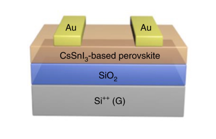
To overcome this issue, the researchers from POSTECH (Pohang University of Science and Technology) in Korea led by Yong-Young Noh and PhD candidates Ao Liu and Huihui Zhu, in collaboration with Myung-Gil Kim of Sungkyunkwan University, used the modified inorganic metal halide caesium tin triiodide (CsSnI3) to develop the p-type perovskite semiconductor and fabricated the high-performance transistor based on this.
This transistor exhibits high hole mobility of over 50cm2V-1s-1, On/Off current ratios of more than 108, and recorded the highest performance among the perovskite semiconductor transistors that have been developed so far.
By making the material into a solution, the researchers succeeded in simply printing the p-type semiconductor transistor as if printing a document. This method is not only convenient but also cost-effective, which can lead to the commercialisation of perovskite devices in the future.
“The newly developed semiconductor material and transistor can be widely applicable as logic circuits in high-end displays and in wearable electronic devices, and also be used in stacked electronic circuits and optoelectronic devices by stacking them vertically with silicon semiconductors,” explained Professor Yong-Young Noh on the significance of the study.
This study was conducted with the support from the Mid-Career Researcher Program, Creative Materials Discovery Program, Next-generation Intelligence-Type Semiconductor Development Program, and the Basic Research Lab Program of the National Research Foundation of Korea, and from Samsung Display Corporation.
REF
'High-performance inorganic metal halide perovskite transistors' by Ao Liu et al; Nature Electronics 17-Feb-2022


