

Superior switching
Data centres and optical networks could benefit from a new generation of
wavelength blockers, formed by uniting the strengths of InP and silicon
photonics
BY NETSANET TESSEMA, KRISTIF PRIFTI, AREF RASOULZADEHZALI, YU
WANG, RIPALTA STABILE AND NICOLA CALABRETTA FROM EINDHOVEN
UNIVERSITY OF TECHNOLOGY AND GIOVANNI DELROSSO, SRIVATHSA
BHAT AND TIMO AALTO FROM VTT RESEARCH INSTITUTE
While many of you know quite a bit about LEDs, lasers and solar cells, it’s possible that you have never heard of the wavelength blocker. Yet despite its low profile, it is produced in high volumes, playing a key role in today’s optical networks, where it provides the smallest wavelength-selective switch.
The deployment of wavelengths blockers is on an upward trajectory, driven by technologies such as 5G, Cloud computing and the Internet of Things. In all these applications, it is essential to efficiently utilize the available bandwidth within the optical fibre network.
In order to understand the role of the wavelength blocker, you must first get to grips with the basics of dense wavelength division multiplexing (DWDM), a technology based on bringing together optical signals at different wavelengths and transmitting all this aggregated information through an optical fibre.
A key component in these networks is the optical add/drop multiplexer (OADM). It taps (that is, drops) information at some wavelengths, while sending it on that at other wavelengths. Another attribute of the OADM is that it can add new wavelengths onto an optical fibre, allowing additional signals to be transported to other destinations.
The first generation of OADMs connected spectral demultiplexers and multiplexers by a fibre patch cord. The downside of this arrangement is that it did not have any capability to be reconfigured – that required manual intervention to change the wavelength dropped or added. This weakness stemmed from employing a fixed wavelength for port mapping in the spectral multiplexing/demultiplexing devices, and resulted in the need to physically disconnect fibre patch cords during reconfiguration. Such a state of affairs is clearly undesirable. It is far better to avoid any manual intervention – and that motivated the migration to a new form of OADM that has dynamic reconfigurability.
This is where the wavelength selective switch (WSS) has a major role to play. Without any manual intervention, this form of switch can forward an incoming wavelength at the input port to one or more output ports of an OADM. This transforms the OADM into a Reconfigurable variant, known as a ROADM. It is this more sophisticated successor that lies at the backbone of today’s high capacity optical network, enabling dynamic transport of traffic in a manner that leads to efficient use of bandwidth and network resources. Note that WSS enables independent switching of any wavelength to any port, without restrictions imposed by the switching of other wavelengths.
An additional role played by the WSS is to provide dynamically reconfigurable connectivity between the switches at the top of the racks within a data centre network. Helping to fulfil this task is a software defined network, which automates provisioning of network resources according to current traffic demands.
Marrying materials
Lying at the heart of a WSS are a number wavelength blockers (WBLs), each with one input port and one output port. Several research groups have demonstrated WBLs using silicon photonics, but they are compromised by a poor on/off switching ratio and a high insertion loss, attributed to a large port count. As this platform does not have the capability to include a gain section that compensates for on-chip power losses, it is not an ideal candidate for implementing a WBL.
Another material for making a WBL is InP. Its strength is that it can compensate for on-chip losses by incorporating semiconductor optical amplifiers (SOAs), which also provide a high on/off switching ratio. But the limited wafer size of InP hampers scaling to a large wavelength and port count.
The best way forward is to adopt a hybrid approach that addresses all the limitations just described. For this architecture, silicon photonics is used for the passive parts – that is, the demultiplexer and multiplexer – and InP is employed to realise gain, forming an SOA that provides on/off switching and amplification. With this combination, scaling up the port and wavelength count draws on the merits of silicon photonics, while InP provides switching with high on/off ratio and amplification.
Our team at Eindhoven University of Technology, The Netherlands, working in partnership with engineers at VTT Research Institute, Finland, has broken new ground by fabricating the first ever hybrid WBL. Collaborating through an EU project named PASSION – its full name is Photonic technologies for progrAmmable transmission and switching modular systems based on Scalable Spectrum/space aggregation for future agIle high capacity metrO Networks – we are taking on the ambitious goal of developing a software-defined network featuring transceiver and switching node technology for high capacity metropolitan optical networks. The goal is to reach a capacity as high as 8 Tbit/s per second per polarization, using 160 wavelength channels within the C-band, with transmission routed down a single fibre.
The motivation for our development of our hybrid WBL is that it can play a crucial part in a scalable and modular WSS for a high capacity switching node within a metropolitan optical network (see Figure 1). This technology is based on a broadcast-and-select scheme, with a WDM signal broadcast by a power splitter and selected by WBL modules at the output ports. To compensate for loss associated with a power splitter, signals can be boosted by an SOA, formed in InP. At each output port of the WSS, a WBL is used to pass or block a wavelength channel by turning gate SOAs on or off respectively. If the port count of the WSS needs to increase, a new WBL switching module is added.

Figure 1. Architecture of hybrid integrated wavelength selective switch
(WSS). A hybrid WSS can be developed with one input port and m output
ports by integrating m hybrid WBL modules. The WBL has 1 to n channel
mapping at the demultiplexer and n to 1 channel mapping at the
multiplexer. There are n SOA switching gates, formed from InP.
Demonstrating devices
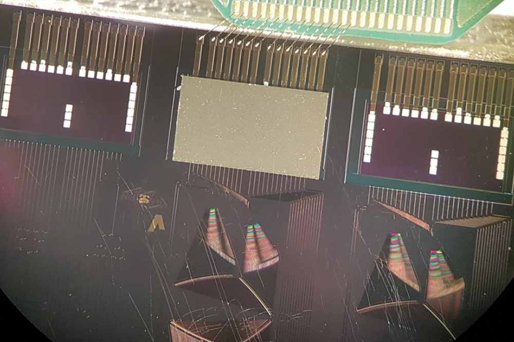
We have demonstrated the proof-of-concept of our hybrid WBL by designing and fabricating a pair of chips on silicon photonic and InP platforms (see Figure 2 for the mask layouts of two 1 x 12 arrayed waveguide gratings formed using silicon photonics and an array of 12 SOA gates on InP). By placing SOA switching gates in a U-shape, we allow input/output straight waveguides to be accessed from the same side. Flip-chip bonding unites the silicon photonics and InP chips, and realizes the hybrid WBL. As well as housing de-multiplexer and multiplexer arrayed waveguide gratings, the silicon photonics chip has a cavity, designed to accommodate the InP chip during flip-chip bonding assembly.

Figure 2. The mask layout of silicon photonics (SiPh) (left) and InP
(right) PIC design for the implementation of a hybrid WBL module with
n=12 wavelength channels (10 functional and 2 test channels). Channel
spacing is 0.8 nm (100 GHz).
In our hybrid chip, waveguides are formed in InP and silicon (see Figure 3). Those formed in silicon, based on VTT’s 3 µm by 3 µm waveguide technology, provide a polarization-insensitive performance that doubles the transmission capacity per wavelength channel – data can be simultaneously transmitted in the transverse electric and the transverse magnetic polarizations. The InP waveguide features a 0.5 µm-thick InGaAsP core. Due to the difference in the size of this core and that in silicon, to ensure that hybrid coupling losses are below 3 dB, when the waveguides are brought together, their air-gap must be less than 2 μm, and the alignment accuracy must be below ± 0.5 μm in the vertical and lateral directions.

Figure 3. Cross-sectional diagrams of SiPh/InP waveguides (top) and a flip-chip assembly process (bottom).
Our flip-chip bonding process involves gold-coated contact pads on the InP chip and tin-coated contact pads on the silicon photonics chip. The two entities are united by thermal compression at an elevated temperature of 220°C. Once bonded, the patterned stopper on the silicon photonics chip provides mechanical support to the InP chip. Use of lithography allows us to vertically align the top contact areas of the silicon photonics mechanical stoppers and the recessed areas in the InP chip (see Figure 4 for images of the: silicon photonics chip with cavities after fabrication; the InP chip aligned to the silicon photonics cavity; and the hybrid WBL switch after assembly).
Flip-chip bonding provides us with a placement accuracy below 0.5 µm in the vertical and lateral directions. However, a limitation of the visual system that we used for bonding is that it prevented us from precisely controlling the airgap between the two chip facets, resulting in an air gap of the order 8 µm; this led to excess coupling losses between silicon photonics and InP waveguides.
Channel characteristics
We have characterized our hybrid WBL electrically and optically. Of the ten wavelength channels, eight are working – they are channels Ch1, Ch3, …, Ch9. The most likely reason that two channels are not working is optical damage at the waveguide facets of the SOAs, occurring during the flip-chip bonding process.

Figure 4. Images of a: fabricated SiPh chip with cavities (top left);
SOA chip aligned into the cavity during flip-chip bonding (FCB) (top
right); InP chip placed into a SiPh cavity (bottom left); and a hybrid
WBL after FCB (bottom right).
Plotting the current-voltage of the SOA gate switches before and after integration shows that the variation in resistance is only 4.5 Ω (see Figure 5). Transmission characteristics of the eight wavelength channels reveal that the typical on-off ratio is around 30 dB (see Figure 6).

Figure 5. Current-voltage curves before and after flip-chip bonding.
After optimally tuning the current for each gate SOA to minimize fibre-to-fibre loss and the effect of back reflection on the hybrid WBL, fibre-to-fibre losses for Ch1, Ch3, Ch6, Ch7, Ch8 range from 32.2 dB to 37.5 dB. Such high losses stem from the large air gap, which needs to be below 2 μm in the horizontal direction to keep hybrid coupling losses below 3 dB. To help address this loss, we plan to move to on-chip integrated spot-size converters, because they relax the tight airgap tolerance. Another improvement we will be making is to introduce angled waveguides – they alleviate the impact of back reflection and fully employ the gain of SOAs.

Figure 6. Transmission characteristics of eight wavelength channels when
SOA gates are turned On and Off for an input optical power of 0 dBm.
Input optical signal (dotted line), output optical signal of the hybrid
WBL switch ON (solid line) /Off state (dashed line).
Investigating the gain characteristics of the gate SOA for Ch3, for varying current and varying input power, has uncovered a significant variation in fibre-to-fibre loss. It varies from 60 dB when the SOA has no drive current and it is in an absorption state, to 26 dB, due to gain provided by the SOA at 100 mA (see Figure 7, and also Table 1, which summarizes the fibre-to-fibre loss of each channel and the corresponding current of the SOA gate).

Table 1. Fibre-to-fibre loss of each channel and the corresponding current of the SOA gate.

Figure 7. Fiber-to-fiber transmission and gain characteristics of a SOA
(Ch3). The fibre-to-fibre loss is of the order of 33 dB at 80 mA for all
input power values. The loss decreases to 26 dB at SOA current of
100mA; for input power of 0 dBm and -5 dBm. Effects of a SOA saturation
on the fibre-to-fibre loss are slightly observed at 100 mA for input
powers of 7 dBm and 10 dBm, resulting fibre-to-fibre losses of 29 dB and
31.57 dB, respectively.
To evaluate data transmission, we have employed a tuneable laser source to generate the wavelengths corresponding to the channels of the WBL, and used 10 Gbit/s NRZ 27-1 and 20 Gbit/s NRZ 23-1 PRBS patterns (see Figure 8). Using 10 Gbit/s signals, measurements of the bit error rate at various received powers produced clearly opened eye diagrams for Ch1, Ch3, Ch6, Ch7, and Ch8 (see Figure 9). Power penalties range from 0.3 dB to 1.5 dB.

Figure 8. Experimental set-up for data transmission at (a) 10 Gbit/s
and (b) 20 Gbit/s. Light is coupled in and out of the hybrid WBL switch
with lensed fibre. To compensate for losses in this switch, input
optical modulated data is boosted by 17 dBm. For the 20 Gbit/s signal,
after light is transmitted through the WBL, it is boosted by a second
preamplifier, so that it is sufficient for the sensitivity of the
receiver. Inserting a bandpass filter with a 3 dB bandwidth of 200 GHz
removes the out-of-band noise of the pre-amplifier. For each channel the
current of the SOA is optimised to minimize power penalties.
When data transmission capacity was increased to 20 Gbit/s, we still observed clear eye diagrams and obtained error-free performance (see Figure 10). Power penalties ranged from 0.7 dB in the case of Ch3 to 2.8 dB in the case of Ch8 (see Table 2 for the power penalty at a bit error rate of 1 x 10⁻⁹).
These results, and those at 10 Gbit/s, showcase the suitability of our modular hybrid WBL for deployment in a high-capacity switching node. For this application, capacity may be scaled by adding new modules in a pay-as-you-grow manner.

Figure 9. The bit error rate (BER) as a function of received power and eye diagram at 10 Gbit/s.
 Figure 10. The bit error rate (BER) as a function of received power and eye diagram at 20 Gbit/s.
The road ahead
Success to date has enabled us to demonstrate a proof-of-concept hybrid WBL module that is based on silicon photonic passives and InP actives. For this we used a flip-chip bonding process to produce just four samples, undoubtedly a small number for such an assembly process. We are now laying the foundations for trimming hybrid coupling loss between the silicon photonic and InP waveguides, and maximizing the yield of the flip-chip bonding assembly process.
Addressing the low loss in our module will unlock the door to a high degree of integration, involving a large port count and wavelength count WSS. In turn, this will equip our device for deployment in current metropolitan optical networks and data centre networks.
For both of these applications, our WBL benefits from the large degree of integration associated with silicon photonics. We can scale the number of wavelength channels per WBL up to 40 and enjoy a wide operating range, thanks to the optical transparency of the silicon photonics VTT waveguide technology through O and L bands. Another strength of our technology is that the SOA switching gates span a substantial spectra range, and can be optimised for O, E, S, C and L bands. This provides multi-band WSS functionality, a major asset in high-capacity metro and data centre networks.
One of the major goals of the PASSION project is to develop technolgy for a software-defined network. This features programmable metro nodes, referred to as Level-1 nodes, designed to meet the agile capacity demands of the metropolitan network (see Figure 11 for an illustration of the metro-core architecture and the details of how this can aid these networks). As the network grows, new WSS modules can be added in the drop and add directions.

Figure 11. In this network, the L1 node is a high-capacity ROADM node,
equipped with colour-less, direction-less, contention-less capability.
This node can transparently switch space-division multiplexed systems
via Fan-out and Fan-in of multi-core fibre bundles. The photonic space
switch handles traffic flow in the spatial domain in the express in/out
path. Incoming express-in traffic is either sent forward directly as
by-pass traffic, or directed to the disaggregate switch in the drop path
as drop traffic. Operating in a similar manner, this switch adds
traffic in the express-out path. The WSS (drop) acts as a disaggregating
switch, while the WSS (add) provides an aggregating switch. Working
together, they offer dynamic reconfigurability. When traffic has a
common destination it is bundled and sent forward in the express-out
path so that, at the next L1 node, express ports transparently direct
the traffic. The L1 node also enables adding/dropping of traffic from/to
the access Level-2 (L2) network, which has L2 nodes with 2-degree
ROADMs based on a WBL and 1:2 splitter and 2:1 combiner. In addition,
there are local add/drop functionalities at the L1 node. They are
embedded at the WSS: in the add directions via sliceable bandwidth
variable transmitters (SBVTs); and in the drop direction via multi-cast
switches (MCS) and coherent receiver modules (CRM).
Our WSS could also have a role to play in data centre networks, which provide full connectivity to thousands of servers hosting various applications, such as cloud computing, big data and IoT. In these networks, optical switches can help to support high bandwidth, and are a promising candidate to replace the electronic switches that struggle in this regard. A move to optical switches can also trim power consumption in these networks by eliminating electrical-optical-electrical conversion, which is essential when using electrical switches.
In data centre networks, WSS are used to create a reconfigurable connectivity between the top-of-the-rack switches (see Figure 12). The technology also enables the introduction of optical top-of-the-rack switches, which create dynamic connectivity within several servers in a single rack. Using our hybrid WBL, switching can take place in few nanoseconds, fulfilling the speed requirements of packet switching needed for broadband operation within the datacentre.

Figure 12. Reconfigurable data center architecture; the WSS is used to
connect top-of-the-rack switches (TORs) within a cluster and several
clusters
While there is still much to do to improve and refine our hybrid chip, by uniting the best attributes of silicon photonics with the strengths of InP, this device clearly has much to offer. 
Table 2. Power penalty at a bit error rate of 1 x 10⁻⁹.


