
EVG and Toppan Photomask partner on nanoimprint lithography
Collaboration will provide nanoimprint lithography development kits and foster industrial-scale implementation
EV Group (EVG), a supplier of wafer bonding and lithography equipment, and Toppan Photomask have entered into an agreement to jointly market nanoimprint lithography (NIL) as an enabling high-volume manufacturing (HVM) process for the photonics industry.
EVG pioneered NIL from a research approach 20 years ago to implementation in volume production on various substrate sizes from 2 inch compound semiconductor wafers to 300 mm wafers and even on large-area panels. Traditional lithography technologies are reaching their limits when it comes to addressing applications that require the creation of small and arbitrarily shaped patterns, such as metalenses.
NIL is a proven, cost-effective process for generating nanometer-scale-resolution patterns on complex structures, and thus is a viable alternative for these applications.
The collaboration aims to establish NIL as an industry standard production process for photonics manufacturing, and accelerate its implementation in HVM to support a wide variety of applications. These applications include augmented/mixed/virtual reality headsets, smartphone and automotive sensors, as well as medical imaging systems.
As part of this non-exclusive collaboration, EVG and Toppan Photomask will pool their knowledge, expertise and services to provide NIL development kits using master templates from Toppan Photomask and equipment and process development services provided by EVG.
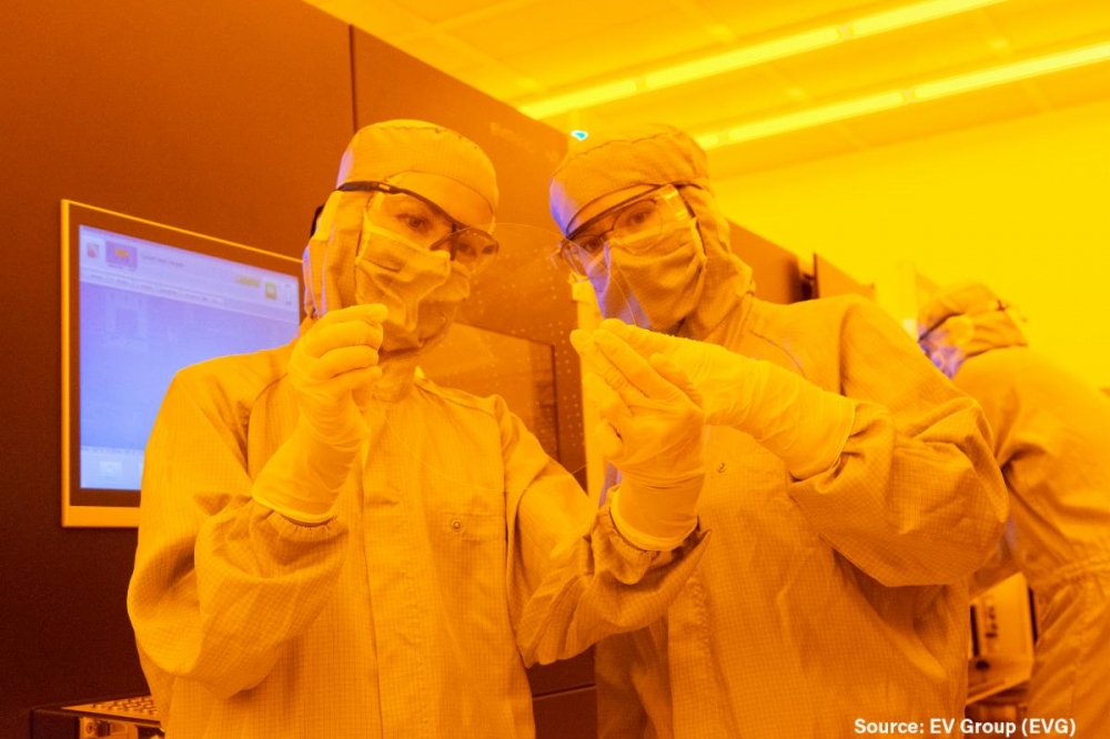
In addition, EVG will offer NIL technology and product demonstrations to interested companies at EVG’s NILPhotonics® Competence Centre at its headquarters in Austria. Furthermore, each company will designate the other as a recommended supply chain partner to companies interested in leveraging NIL to support their production needs.
“Toppan Photomask is very excited to enter into a collaboration with EVG”, said Chan-Uk Jeon, chief technology officer of Toppan Photomask Co., Ltd. “EVG’s NIL tooling and processing capabilities are world class and will enable cost-effective growth in photonics and other new technologies that are now adapting to NIL technology. Toppan Photomask sees a bright future as NIL grows into another successful lithography solution, enabled by both companies’ established strengths.”
According to Markus Wimplinger, corporate technology development and IP director at EV Group, “We are excited to be partnering with Toppan Photomask to bring nanoimprint lithography to mainstream manufacturing applications. As the leading supplier of semiconductor photomasks with a reputation for the highest-quality standards, Toppan Photomask has extensive experience working with standardised production methods involving the world’s most stringent manufacturing requirements. This first-of-its-kind collaboration between a nanoimprint process equipment and services provider and a nanoimprint master manufacturer is a huge win for the industry and will aid our customers in quickly scaling up NIL as a mass-production technology for advanced optical devices and components – helping them to bring new ‘virtual’ ideas into reality.”
Experts from both companies will be available to discuss this collaboration at the Micro and Nano Engineering (MNE) Eurosensors 2022 Conference, taking place at the Gasthuisberg academic campus in Leuven, Belgium, from September 19-23.
In addition, Christine Thanner of EVG is giving an invited plenary talk at the Nanoimprint and Nanoprint Technology (NNT) Conference in Toyama, Japan on October 5, titled “Nanoimprint – from niche to high-volume manufacturing,” where she will address the importance of having a matching combination of NIL mastering techniques, replication equipment and processes.


