

Advancing Ga2O3 doping
Nitrous oxide, ammonia, and several carbon-containing molecules are strong contenders for doping gallium oxide. But which one’s the best?
BY FIKADU ALEMA, AARON FINE, WILLIAM BRAND AND ANDREI OSINSKY FROM AGNITRON.
There’s a lot to like about Ga2O3. Thanks to a bandgap of around 4.8 eV, this semiconductor promises to provide more efficient switching than today’s rising duo, SiC and GaN. What’s more, crystals of Ga2O3 can be formed from the melt, indicating the potential for low-cost production of ultra-wide bandgap devices.
However, the picture is not all rosy. In addition to concerns over a limited thermal conductivity for Ga2O3, there are significant issues associated with doping [1].
Today it seems that the chances of effective p-type doping in Ga2O3 are rather bleak, due to the small energy dispersion of the valance band and the large effective masses in valance band states. These inherent weaknesses are limiting Ga2O3 device architectures to those that are unipolar. Although researchers have investigated whether impurities such as magnesium, iron, and nitrogen could unlock the door to p-type conductivity, all attempts resulted in deep acceptors.
Such efforts are still valuable, though, because deep acceptors are beneficial for engineering Ga2O3 power devices. When Ga2O3 substrates are not intentionally doped, they still exhibit unintentional n-type conductivity, associated with significant levels of silicon, a background impurity. One can compensate for this by adding acceptor impurities, such as magnesium or iron, to the Ga2O3 melt – this enables the production of semi-insulating or highly resistive β-Ga2O3 substrates. The addition of deep acceptor impurities causes the equilibrium Fermi level to move away from the conduction band edge and closer to acceptor dopant states. This shift in the Fermi level allows a junction to form with adjacent n-type material, thus opening the door to the realization of potential barriers for voltage blocking. Ultimately, this could enable enhanced-mode Ga2O3 MOSFETs with an accepter-doped channel.

Figure 1. SIMS depth profiles for nitrogen and hydrogen in a Ga2O3 SIMS stack of layers doped using NH3/N2 as a source for nitrogen doping. The A, B, C, and D labels show layers grown by introducing ammonia flow rates of 0.8, 4, 6, and 30 sccm. Increasing ammonia flow rate increases the nitrogen and hydrogen incorporation into the films.
Silicon does not just play a role within the layers of Ga2O3. In addition, as shown by secondary-ion mass spectrometry (SIMS), this element accumulates at the interface between the epitaxial film and substrate, regardless of growth method, process conditions, and the dopants in the substrate. The presence of silicon, thought to originate from silica-based polishing of the substrate, is a nuisance, degrading device performance. For example, in Ga2O3 FETs, silicon accumulating at the substrate-epilayer interface gives rise to a parasitic conductive channel that prevents the device from pinching off.
At Agnitron Technology, a provider of MOCVD tools for Ga2O3 growth based in Chanhassen, MN, we are fully aware of these issues and are playing our part in addressing them. We see ourselves as far more than simply an equipment supplier – we are heavily involved in developing Ga2O3 growth and processing technology, and through our collaborations with many leading research groups, we are helping to uncover solutions to many of the challenges associated with intentional doping of this oxide, as well as combating the impact of unwanted impurities. We shall offer a flavour of our success, and that of others, in the remainder of this feature.

Figure 2.Linear dependence of the nitrogen and hydrogen incorporation on the molar flow rate of ammonia diluted in nitrogen (NH3/N2).
Excelling through etching
One common approach to trimming the concentration of silicon at the epilayer-substrate interface is to etch the Ga2O3 substrate in concentrated HF acid for around 30 minutes prior to growth. While this step does not eradicate silicon at the interface, its concentration falls. This leads to partial compensation by the acceptor impurity – either magnesium or iron – that defuses into the film/substrate interface from the semi-insulating substrates during epitaxial growth. Device results show that this methodology thwarts the threat of interfacial silicon reaching the active channel of the device. Working in partnership with Krishnamoorthy’s group from the University of California, Santa Barbara (UCSB), last year, we reported high-performance, multi-kilovolt class Ga2O3 MESFETs with a record figure-of-merit for power of more than 350 MW/cm2 [2].
As 30 minutes of etching fails to remove all interfacial silicon, it is tempting to increase the time for this process. But that’s not a good idea: HF damages the substrate’s surface, resulting in rough epitaxial films with surface pits that impair device performance. A far better approach is to compensate the interface with deep acceptor dopants, by either modifying the growth process or by ion implantation.
The merits of MOCVD
Of these two options, a growth-based approach delivers far better results. Implanting the likes of magnesium, nitrogen and iron requires an ion beam with such a substantial energy that it damages the crystal structure of Ga2O3 material and introduces unintended defects [3]. While thermal annealing can repair crystal quality, it causes impurities to defuse and redistribute inside and outside the implanted area. That’s an impediment to realising a uniform, sharp doping profile.
Both MOCVD and MBE can provide uniform lateral and depth doping with no additional post-growth treatment. For MOCVD, researchers have demonstrated doping of Ga2O3 with magnesium, nitrogen and iron deep-acceptor dopants. Of the three, the two cation site acceptor species in Ga2O3– that’s iron and magnesium – have received more attention, partly because of their success in GaN. These dopants can be added using Cp2Fe and Cp2Mg, precursors that are solid at room temperature and have a low vapor pressure [4, 5]. Molar flow rates control doping concentrations.
For both these precursors, process engineers must deal with a surface riding issue. There’s a threat that during the growth, doping extends into the layers not intended to be doped. This is exacerbated when a high substrate temperature is employed for the growth of the films [6, 7].
We have spearheaded efforts to develop doping by nitrogen, as this approach is less affected by thermal diffusion. Doping by nitrogen, which realizes deep acceptor conduction by substituting the oxygen site in Ga2O3 [8], can be realised with various nitrogen sources, including nitrous oxide (N2O) and diluted ammonia. Note that molecular nitrogen (N2) is unsuitable, due to its high level of stability that prevents the production of active nitrogen species for doping.
Nitrous oxide or ammonia?
The primary use of N2O is as an alternative oxygen source for MOCVD of Ga2O3. Note that switching to this is not trivial, requiring an entirely different set of growth conditions to those typically used for growth with pure oxygen, including a higher growth pressure and temperature to ensure efficient decomposition of this oxide [7]. When used for both the growth of Ga2O3 and its nitrogen doping, the incorporation efficiency of nitrogen depends on process conditions, such as the N2O/III ratio, substrate temperature, and chamber pressure. By varying these process conditions, β-Ga2O3 films with a nitrogen concentration ranging from an undetectable level up to around 2×1019 cm-3 have been realised, according to SIMS. Increasing the growth temperature decreases the concentration of nitrogen, but its incorporation is accompanied by hydrogen, which follows a similar profile [5-7].
Films grown with an undetectable nitrogen concentration have also shown room-temperature mobility of more than 150 cm2 V-1 s-1, with a low free-carrier concentration of around 2 × 1014 cm-3. Realising a low free-carrier concentration, alongside a mobility that’s comparable to that for material grown using pure oxygen, is vital for high-voltage vertical power devices. Unfortunately, the purity of the N2O-grown film is inferior to that grown using pure O2, according to a low-temperature Hall measurement. This is thought to probably be associated with high compensation, related to nitrogen in the film, despite this element being undetectable by SIMS. At room temperature, the Hall mobility is not affected by nitrogen, because phonon scattering is the dominant mechanism.
The incorporation of hydrogen in the epilayers is far from ideal, because it acts as a shallow donor, compensating nitrogen [9]. This concern, alongside a high level of sensitivity of nitrogen incorporation to process conditions, makes it challenging to realise controllable doping. This led us to explore an alternative dopant, ammonia, which is widely used for the growth of GaN-based devices. Besides, ammonia decomposes at a relatively low substrate temperature of around 600 °C, making it a good candidate for use in nitrogen doping without altering typical growth conditions for Ga2O3 – that’s not the case when using N2O.
One of the key advantages of using ammonia, rather than N2O, is that the flow rate can control the concentration of nitrogen incorporated in the film (see Figure 1). The relationship is ideal, with the nitrogen concentration linearly increasing with the molar flow rate of ammonia (see Figure 2).
Unfortunately, when ammonia is employed as a precursor, the level of hydrogen tracks the nitrogen profile when films are formed at a typical growth temperature for Ga2O3. Moving to a higher growth temperature is beneficial: this increases the pyrolysis efficiency of ammonia, and when this gas is used to dope Ga2O3 films at these elevated temperatures, this reduces the hydrogen concentration, according to SIMS. Growing the film at a 100 °C higher than the typical growth temperature led to a reduction in hydrogen concentration by a factor of around 7. Annealing at elevated temperatures in a reduced-pressure environment may offer another approach to reducing the hydrogen concentration in these films, but its presence could still lead to compensative behaviour for nitrogen.
Our experiments back this up. We grew a number of nitrogen-doped single-layer Ga2O3 films with nitrogen concentrations of more than 2 x 1018 cm-3. All samples were very resistive, with values for resistance more than three orders of magnitude higher than the control sample, an unintentionally doped Ga2O3 film produced under the same growth conditions. It is possible that hydrogenated gallium vacancies also lead to the electrical passivation of hydrogen [10].
Based on these findings, we feel that now is the time to explore an alternative precursor for the growth of nitrogen-doped, hydrogen-free Ga2O3 films. Our plan is to investigate nitric oxide (NO).

Figure 3. SIMS depth profiles for carbon in a Ga2O3 sample doped from TMGa by adjusting the O2/TMGa ratio. The carbon concentrations increase with the decrease in the O2/TMGa ratio, as seen from the inset.
Carbon doping
In materials such as GaN, when carbon provides the dopant, it is known to act as a deep acceptor. However, how carbon behaves in Ga2O3 is far less clear. Some predict that it acts as a deep DX centre [11], while others argue that it behaves as a positively charged shallow donor [12].
There are several candidate materials for realising carbon doping during MOCVD. One option is to introduce simple hydrocarbons into the reactor, such as propane, but there is also the possibility of carbon doping with the precursor trimethylgallium (TMGa), which is used for film growth. A commonly cited challenge associated with the use of TMGa for the growth of Ga2O3 is a massive carbon incorporation into the growing layers, resulting from highly reactive methyl radicals forming during the pyrolysis process. However, the extent of this carbon incorporation is governed by process conditions – primarily the ratio of oxygen to TMGa. Adjusting this allows the growth of Ga2O3 films that are either doped or undoped with carbon.
We have used our family of Agilis MOCVD reactors to study the role that the ratio of oxygen to TMGa plays in carbon incorporation (see Figure 3). This involved growing a stack of layers at a constant pressure and substrate temperature, but varying the VI/III (oxygen to TMGa) ratio. According to SIMS, when we increased the VI/III ratio from 170 to 1220, this led to an almost linear fall in carbon incorporation by two orders of magnitude – it fell from around 2 x 1019 cm-3 to around 2 x 1017 cm-3.
Working in partnership with researchers at the Air Force Research Laboratory, we have investigated films grown using oxygen-to-TMGa ratios beyond 2000. This created films that are essentially carbon-free – if there is carbon incorporated, it is beyond the SIMS detection limit of around 6 x 1016 cm-3 – with record high low-temperature mobility of more than 23,000 cm2 V-1 s-1 and an acceptor concentration of as low as 2 x 1013 cm-3 [13].
Our studies have shown that adjustments to the reactor pressure and the substrate temperature have no effect on carbon incorporation. This is evident from our growth of a number of layers at different pressures and temperatures, using a VI/III ratio in excess of 2000. Measurements of these test samples by SIMS show that the carbon content in the films remains below the instrument’s detection limit. This has led us to conclude that the way to control the concentration of carbon in Ga2O3 films is to adjust the ratio between oxygen and TMGa.
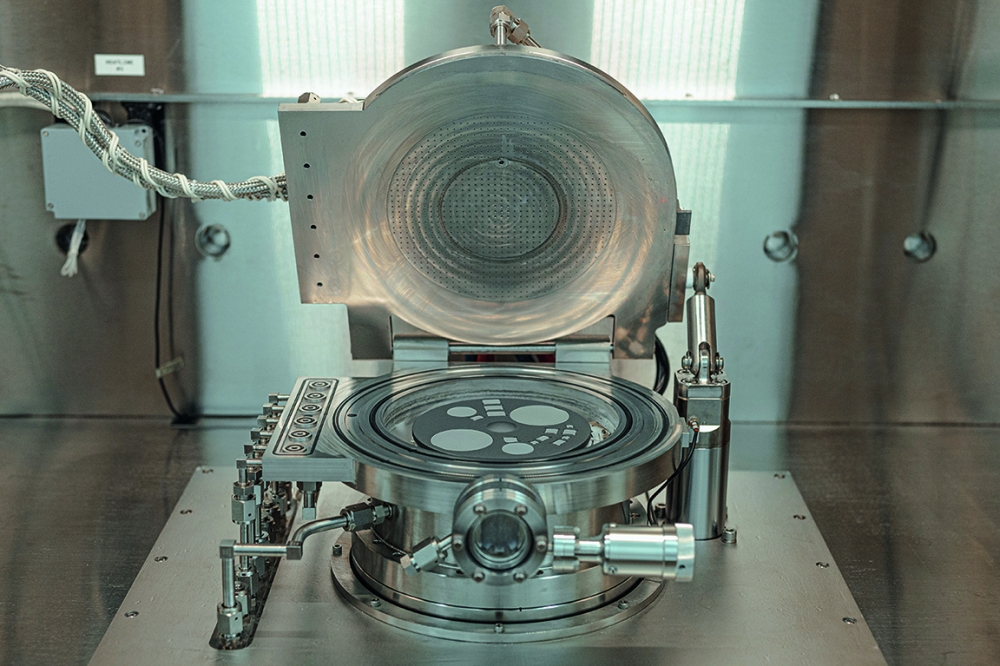
 Agilis 500 MOCVD reactor from Agnitron with an open showerhead and
wafers with various shapes and sizes loaded onto the wafer carrier.
Agilis 500 MOCVD reactor from Agnitron with an open showerhead and
wafers with various shapes and sizes loaded onto the wafer carrier.
Building on this investigation, we have explored the electrical properties of Ga2O3 films co-doped with carbon and silicon. Using O2/TMGa ratios employed for the work presented in Figure 3, we have produced films and measured their room-temperature and low-temperature mobilities, using the Hall method. This investigation showed that for concentrations of carbon below 2 x 1017 cm-3, the level of this dopant has no impact on mobility; but when this increases from this limit by an order of magnitude, mobility diminishes significantly (see Table 1). At higher carbon concentrations, there is more substitution on the gallium site, leading to crystal distortion and electrical compensation – both impact room-temperature and low-temperature mobilities.

Table I: Electrical characteristics of carbon-doped films grown by varying the O2/TMGa ratio.
While there is still much progress to be made, our efforts show that there are many different approaches to doping Ga2O3. Results depend on both the choice of dopant and the growth conditions.
The works discussed in this article were in large part funded by Office of Naval Research (ONR) through STTR Phase II program, contract number N6833518C0192, under the direction of Mr. Lynn Peterson. Agnitron also acknowledges Professors James S. Speck and Sriram Krishnamoorthy – both from UCSB – for their support and collaborative contributions which have been important to β-Ga2O3 related progress for the Agnitron team.

Agilis 500 MOCVD from Agnitron that accommodates wafers with various shapes and sizes.
Agnitron's MOCVD portfolio
The experimental results reported in this feature have been
obtained using β-Ga2O3 MOCVD systems made by Agnitron.
This original equipment manufacturer is proud to have had its MOCVD systems
play a crucial role in the majority of scientific journals and conference
presentations – more than 100 – associated with developing β-Ga2O3
materials and devices. Agnitron’s contribution to all this success underscores its
expertise in producing innovative and reliable β-Ga2O3 MOCVD
systems.
At the heart of every Agnitron Ga2O3 MOCVD reactor is a proprietary, high speed Rotating Disc Reactor (RDR) vertical growth chamber with additional capabilities allowing for high speed operation – speeds over 1300 revolutions per minute. Through material science and design engineering, deposition throughout the chamber is less apt to find its way to the wafer surface. The unique feature of the high-speed RDR is its flow dynamics that repress particle recirculation, leaving areas above the wafer clean and free of deposition.
The remote injection gas delivery system has an unintentional gas phase reaction, resulting from the increase in the injection distance to the wafer, leaving undesirable particles on the growing surface of the films. This is due to the high oxidation rate during β-Ga2O3 growth, thus making it very difficult to utilize a remote injection gas delivery system, because the process generates particles that are hard to avoid. If particles reach the wafer surface, they can compromise device performance.
Agnitron addressed this concern by introducing high-speed rotation. With this refinement, particles are carefully managed on the surface and unwanted precipitation is eliminated. However, the excess gas phase reaction owing to the distance to the wafer remained a challenge.
Agnitron countered this threat by using a close-injection gas distribution system that combines the elimination of particles with excellent mixing of gases and precursors. High-speed RDR along with a close-injection gas delivery system reduces the formation of excess particles and prevents unwanted particles from reaching or sticking to the surface of the wafer.
Another merit of RDR high-speed rotation is its higher degree of control, ensuring superior thickness distribution uniformity.
Many of Agnitron’s systems offer tremendous flexibility, allowing the operator to switch between a remote- and a close-injection gas distribution configuration in a matter of hours. Agnitron also offers the capability to add an upgraded close-injection gas distribution system, which ensures even oxygen injection across the entire wafer carrier, rather than just centrally.
Thanks to increasing interest in Agnitron’s β-Ga 2O3 reactors, all its systems are now capable of MOCVD growth on wafers up to 4-inch in diameter. For even larger single wafers, there is the Agilis 500/700
References
[1] J. L. Lyons, "A survey of acceptor dopants forβ-Ga2O3," Semicond. Sci. Technol. 33 05lt02 (2018)
[2] A. Bhattacharyya et al. "Multi-kV Class β-Ga₂O₃ MESFETs With a Lateral Figure of Merit Up to 355 MW/cm²," IEEE Electron Device Lett. 42 1272 (2021)
[3] M. H. Wong et al. "Acceptor doping of β-Ga2O3 by Mg and N ion implantations," Appl. Phys. Lett. 113 102103 (2018)
[4] Z. Feng et al. "Mg acceptor doping in MOCVD (010) β-Ga2O3," Appl. Phys. Lett. 117 222106 (2020)
[5] F. Alema et al. "Low 1014 1/cm3 free carrier concentration in MOCVD grown epitaxial β-Ga2O3" APL Mater. 8 021110:1-9 (202).
[6] F. Alema and A. Osinsky, "Metal Organic Chemical Vapor Deposition 1 – Homoepitaxial and heteroepitaxial growth of Ga2O3 and related alloys " in Gallium Oxide - Materials Properties, Crystal Growth, and Devices, M. Higashiwaki and S. Fujita, Eds. 293 Cham, Switzerland: Springer, 2020, p. 141.
[7] F. Alema et al. "MOCVD Growth of β-Ga2O3 Epitaxy," in β-Ga2O3: Wide-bandgap Semiconductor Theory and Applications, J. S. Speck and E. Farzana, Eds.: American Institute of Physics, 2022.
[8] H. Peelaers et al. "Deep acceptors and their diffusion in Ga2O3," APL Mater. 7 022519 (2019)
[9] J. B. Varley et al. "Oxygen vacancies and donor impurities in β-Ga2O3," Appl. Phys. Lett. 97 142106 (2010)
[10] J. B. Varley et al. "Hydrogenated cation vacancies in semiconducting oxides," J. Condens. Matter Phys. 23 334212 (2011)
[11] S. Lany, "Defect phase diagram for doping of Ga2O3," APL Mater. 6 046103 (2018)
[12] J. L. Lyons et al."Carbon as a Shallow Donor in Transparent Conducting Oxides," Phys. Rev. Appl. 2 064005 (2014)
[13] G. Seryogin et al. "MOCVD growth of high purity Ga2O3 epitaxial films using trimethylgallium precursor," Appl. Phys. Lett. 117 262101 (2020)


