
Optimising fabrication of the GaN-on-silicon HEMT
AlN layers with delayed coalescence provide a great foundation for realising GaN-on-silicon HEMTs with minimal RF loss
The GaN-on-silicon HEMT has its pros and cons: it majors on the use of large, low-cost substrates, and the opportunity to process epiwafers into devices in existing CMOS foundries; but it can suffer from RF loss, stemming from residual metallic atoms diffusing into the substrate during MOCVD growth of the AlN seed layer, which is added to prevent gallium-silicon melt-back at high temperatures.
Fortunately, RF loss can now be addressed in an efficient manner, thanks to a team from China that has developed a CVD process for forming templates that feature an AlN layer with delayed coalescence.
According to this team – a partnership between researchers at Peking University, Jimei University and the Collaborative Innovation Centre of Quantum Matter – their approach is more favourable than the more common one for ensuring that devices don’t suffer from substantial RF loss, involving the cleaning and baking of an MOCVD reactor prior to GaN growth. The engineers argue that by introducing an AlN layer that’s grown ex situ by PVD, it is possible to increase the productivity of GaN-on-silicon MOCVD growth.
The approach of using ex situ growth on sapphire is very mature, with sputtered and PVD growth of AlN on sapphire applied to the fabrication of LEDs. However, it is challenging to realise high-quality, crack-free layers of GaN on silicon substrates with a sputtered AlN interlayer. Compared to in situ growth of GaN on AlN, the defect densities in the GaN that’s grown on ex situ sputtered AlN is an order-of-magnitude higher, and the surface morphology rough, due to the three-dimensional growth mode.
To address the shortcomings of growth on silicon, the team from China turned to PVD, first depositing large AlN nuclei with a low density, before adding GaN via a three-dimensional growth mode that delayed coalescence, key to realising a crack-free epilayer.
Trials to establish a good process involved PVD of a 200 nm-thick AlN layer on 2-inch silicon (111), using an RF power of 200 W or 500 W at 1000 °C, followed by transfer of these samples to an Aixtron close-coupled-showerhead MOCVD reactor, employed for growing buffer-free GaN with a total thickness of 1.5 µm. Structures were formed using both three-dimensional and two-dimensional growth modes, realised using low and high V-III ratios, respectively.
The only crack-free sample, which also had the best crystal quality according to X-ray diffraction, came from the use of a low RF power in the growth of AlN by PVD, followed by the combination of three-dimensional and two-dimensional growth, with a coalescence thickness of 1200 nm.
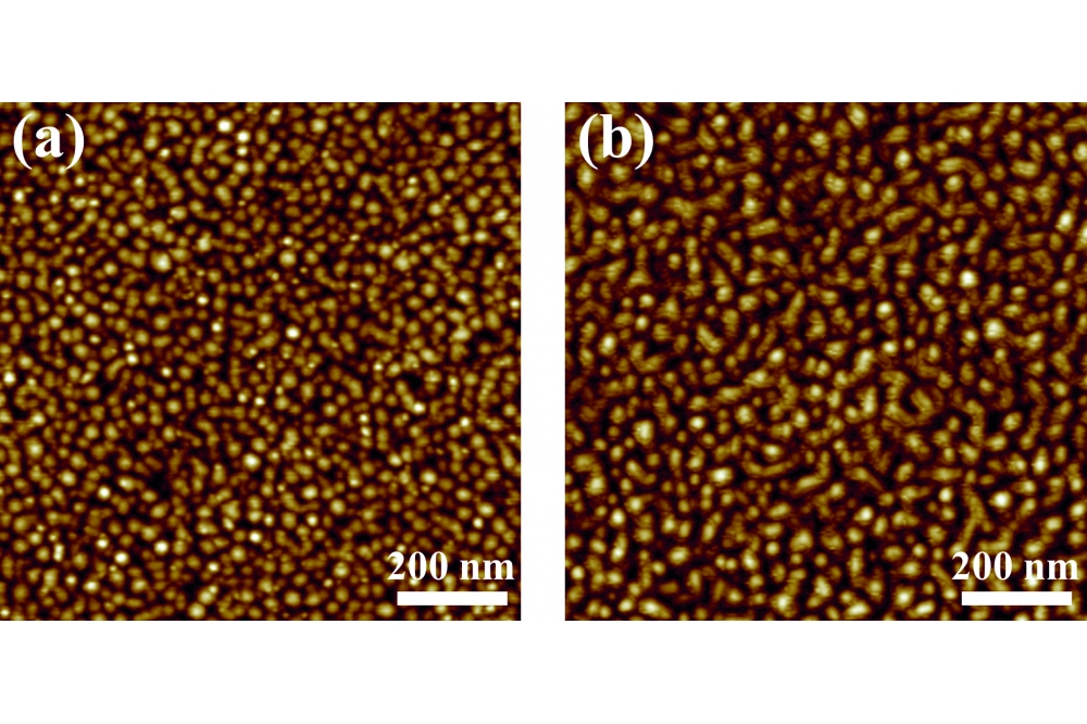
Atomic force microscopy revealed that reducing the RF power from 500 W to 200 W increased the average size of the AlN nuclei from 20-30 nm to 30-50 nm, and halved their density (see picture above).
The team argued that a high coalescence thickness is crucial for managing the stress in the GaN wafer, and preventing cracking. When there is fast coalescence, leading to a low coalescence thickness, there is insufficient compressive stress to compensate for the tensile strain comes that stems from the thermal mismatch between GaN and silicon during cooling.
Spokesman for the team, Xuelin Yang from Peking University, told Compound Semiconductor that further investigations are needed to uncover the optimal conditions for delayed coalescence growth, with efforts needing to consider a greater range of powers for the PVD process and alternative III-V ratios.
Yang thinks that increasing the coalescence thickness and/or the total thickness will improve the crystal quality of GaN. The team measured an RF loss of 0.2 dB mm-1 at 10 GHz, using transmission lines in a coplanar waveguide. This loss is said to be amongst the lowest values reported for GaN-on-silicon.
Targets for the team are to further investigate optimal growth conditions, so that they can realise thicker GaN films with better quality, and to grow AlGaN/GaN heterostructures for the fabrication of HEMT structures.
Reference
D. Liu et al. Appl. Phys. Express 15 081001 (2022)


