

Hitting the road running
The world’s first dedicated, open, pure-play 150 mm SiC wafer foundry
offering a fast route to market has already established a rapidly
filling order book.
BY DAVID CLARK AND RAE HYNDMAN FROM Clas-SiC
As demand for SiC devices and materials continues to grow, there is much need for SiC wafer foundry services. Helping to address this is our team at Clas-SiC Wafer Fab, the UK’s only production volume SiC wafer foundry. Our activities span ‘process design kit (PDK)’ orders – including MOSFETs, junction barrier Schottky (JBS) diodes and merged p-i-n Schottky (MPS) diodes – to recent collaborative projects with major automotive industry players. Within those activities, we are continuing to enhance our capabilities, to ensure our market leadership in technology, quality, and speed. All of this is being realised with impeccable timing – just as the market for SiC power devices is taking off.
The origins of our company can be traced back to the vision of our founder, CEO and former Chairman of the Board of II-VI, Carl Johnson. In 2017 he led the incorporation of our company, which has been founded to provide a ready-made capability for rapid prototyping of new SiC devices in a low-to-medium-volume wafer fab. By succeeding in this endeavour, we are enabling new market entrants to make a speedy journey from custom device design to device fabrication, aided by our established and experienced team offering proven technology.
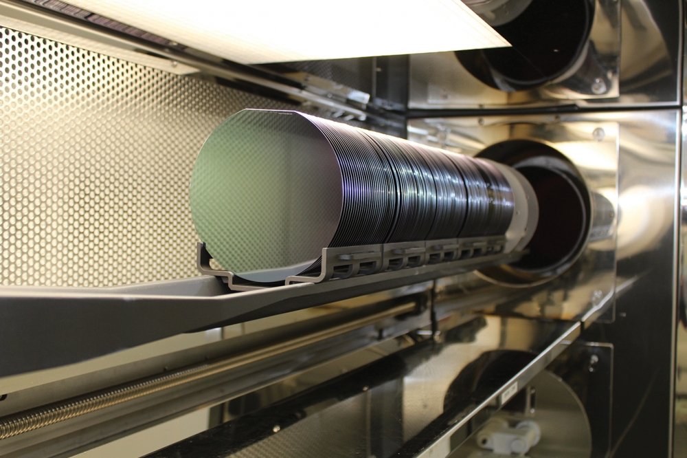
Since our founding we have made great progress, beginning with the construction, from scratch, of a SiC-dedicated wafer fab in Lochgelly, a town located on the outskirts of Edinburgh. The nucleus of our management and engineering team has come from a nearby wafer fab that closed in 2017. Over 30 years that 100 mm fab manufactured millions of silicon devices for high-reliability automotive, rail, fire safety, and medical applications – and from 2004 it processed SiC wafers. With full qualification to ISO9001 and ISO TS16949 standards, that 100 mm fab has equipped us with a unique, experienced pedigree – qualities rarely found in a start-up.
Due to this envious heritage, our company is more re-start than start-up, but from the ground up, in a new facility with new tooling.
Even so, we still had to build a new wafer fab from scratch. That’s a major undertaking, which began by identifying and procuring suitable industrial units. Significant new-build expansion followed, providing additional cleanroom space and facilities that enabled us to almost double our original floor space. We have populated this with brand-new facilities, meeting all modern safety standards. These facilities support the tool set and meet the ISO class 5 cleanroom requirements for SiC device fabrication. Started in 2017, we completed this project in 2019.
A full tool set
During our build we made rapid progress relating to the detailed specifications for, and procurement of, our wafer fabrication tool set. We decided to adopt a large number of tools from the silicon industry, employing well-known ‘workhorse’ equipment from previous silicon technology nodes. Many of these tools are supported by local vendors, from what was once fondly known as ‘Silicon Glen’. We have upgraded these tools so that they can handle transparent SiC substrates, rather than the highly-reflective silicon substrates they were designed to process. We have also made significant investment in additional SiC-specific tooling, including a state-of-the-art high-temperature SiC ion implanter, and a high-temperature implant annealing furnace. This has given us the capability to fabricate SiC power devices from incoming epiwafers, using processes that include wafer-thinning, backside-metallisation and laser-annealing.
We also made investment in wafer-level testing such that we can carry out blocking tests up to 10 kV and conduction-mode tests up to 500 A. Our state-of-the-art testers and automatic probers facilitate rapid testing. We also have reliability testing ovens for high-temperature reverse-bias and high-temperature gate-bias (HTGB) tests that validate our processing platforms.

Figure 1. Clas-SiC offers Process Design Kits to customers, enabling
them to successfully produce custom devices on diode and MOSFET
platforms.
Following our tool procurement, we entered a comprehensive engineering phase involving tool acceptance, qualification and formal certification. We demonstrated planar SiC Schottky diode capability in 2020, followed by the more difficult demonstration of the planar MOSFET capability early in 2022.
Our philosophy has been to employ a reference 15 A, 1200 V MPS diode and a reference 80 mΩ, 1200 V MOSFET as the two vehicles to demonstrate the functionality and reliability of our process platforms. Both reference device types have successfully completed a full suite of rigorous, JEDEC-like reliability testing (see Table 1 for details). Drawing on this proven technology, we have assembled and published PDKs. Our customers are using them to produce custom devices on our diode and MOSFET platforms (see Figure 1 for a summary).

Table 1. Tests on a reference 15 A, 1200 V MPS diode and a reference 80
mΩ, 1200 V MOSFET demonstrate the functionality and reliability of
Clas-SiC’s process platforms.
Speeding to market with PDKs
Designers using our 1200 V MOSFET PDK are able to employ their full innovation to customise the active area of their devices. We provide a 1200 V termination scheme, along with all the processing details. To assist the designer, our PDK includes a Design Rule Manual and Design Rule Check deck.
The PDK is incredibly flexible. It has even allowed one designer to successfully embed multiple sensors within their MOSFETs.
A common customer strategy is to design a multi-project wafer (MPW) mask set. This allows simultaneous fabrication and assessment of many design variations, such as planar, orthogonal and hexagonal architectures.
Thanks to our comprehensive offering, all processing takes place on a common platform, with standard processes and modules. This results in minimal non-recurring engineering and rapid fabrication of prototype MOSFETs. These devices can be produced within twelve weeks, providing customers the advantageous position of a faster route to market.
Our JBS/MPS diode PDK is even more flexible. Offering 1200 V termination, our diode PDK has also been used to design devices across the 650 V – 3300 V range with fully-customised, high-voltage termination schemes. Like the MOSFET, manufacture takes place on a common processing platform, using standard processes and modules.
This results in minimal non-recurring engineering and a direct, reliable route for diode prototype fabrication within just eight weeks.
We have also demonstrated 1700 V and 3300 V MOSFET technologies. Alpha-level PDKs are now available, and full 1700 V and 3300 V MOSFET PDK releases will follow once reliability testing is complete.
It should be noted that standard processes and modules underpinning our PDKs can and have been used with other process technologies. This facilitates rapid fabrication of highly-customised devices, with minimal non-recurring engineering.
By employing PDKs, we can preserve our position as a pure-play foundry, with a clear division of Intellectual Property (IP). Process IP remains with Clas-SiC, while design IP strictly belongs to our customers.
Tool and materials suppliers are interested in our reference devices, using them to investigate new concepts. One example of this is our collaboration with Oxford Instruments, which used our reference to validate a contactless SiC plasma polish approach that could supersede chemical-mechanical polishing. This partner appreciates our support, with company Technical Marketing Manager, Grant Baldwin, describing the project as a ‘fantastic collaboration’.
Future plans
Due to the high level of interest in our SiC PDKs, we are enjoying a steep increase in customer demand.
Buoyed by this we recently doubled headcount to more than 50, and we have plans under way to double again. Running in parallel, our ISO9001 certification is actively under way, with ISO TS16949 qualification planned for 2023. Additionally, we are undertaking an equity-investment round, instigated to fund demand-driven expansion of our capacity by a factor of 2.5 and enhance operational resilience, all on the existing facility footprint.
We have a great deal to look forward to, including exciting volume projections from current and prospective customers.
To fulfil our obligations when these projections come to fruition, we are actively engaging with potential SiC wafer fab partners that are capable of handling high-volume, capacity-hungry customer products. When those products outgrow our capacity, we will hand over to our partners that will be ready to provide high-rate-production capabilities.
From our outset, we have never had any intention of treading water. Our next goals include: qualifying 1700 V and 3300 V MOSFET platforms; continual, incremental refinements to our existing 1200 V MOSFET PDK; continuing to work with our design partner to develop a second-generation 1200 V MOSFET PDK that will enable a significant reduction in MOSFET specific on-resistance while enhancing short-circuit withstand times; and the development of a planar JFET platform, to be launched later this year.
We closely follow technology trends. Observing them has led us to decide that high-voltage devices and trench-MOSFET technology are the next areas for our development programme. This will enable us to offer PDKs for highly customised applications that leverage these advanced technologies. Our customers’ needs dictate our roadmap, and will continue to do so.
Viewpoint: Clas-SiC founder Carl Johnson
I have been involved in compound semiconductors all my working life. Back in 1971, it was clear to see that the II-VI compound semiconductor materials CdTe, ZnSe and ZnS – along with the elemental semiconductor material diamond and the compound semiconductor material SiC – would be the workhorse optical and electro-optical materials in the infrared region of the electromagnetic spectrum. Based on this view, I co-founded II-VI Incorporated to explore, manufacture and supply the highest quality versions of these selected materials.
In 1998, we awakened to the fact that SiC would become an important electronic material, so II-VI launched an effort to become an important supplier of high-quality 6H and 4H-SiC substrates. II-VI initially supplied 2-inch diameter substrates in 2000, before progressively increasing the size. In 2016 II-VI demonstrated the first 200 mm substrates.
The story of my founding of Clas-SiC dates back to March 2017, when I heard that a company in Glenrothes, Scotland, planned to shutter its silicon/SiC wafer fab. I was on the next flight to Edinburgh. I knew it would be synergistic to hire the highly skilled, experienced team of former employees to establish a rapid prototyping and low-to-medium rate production wafer fab to serve the plethora of fabless SiC power device innovators that were soon to be our customers.
At the outset, Clas-SiC adopted a time-tested set of seven values that I helped to establish at II-VI. These values, which have guided decision making and culture at Clas-SiC since its inception, are:
Customers first
⊕ Honesty and integrity
⊕ Open communication
⊕ Teamwork
⊕ Continuous improvement and learning
⊕ Manage by the facts
⊕ A safe, clean, and ordered workplace
We value all our employees. We strive to maintain an environment that offers every one of them an opportunity to grow as fast as they choose, relative to their skill sets and shouldering of responsibility.
Virtually all employees have had the opportunity to become shareholders at Clas-SiC via stock option awards upon the achievement of company-wide goals, or the occasional offer to purchase shares from other shareholders. We believe that employee ownership in a start-up like Clas-SiC is a ‘once-in-a-lifetime’ opportunity, whose value and benefits should not be underestimated by either the employees or their company.
Why SiC is such a big deal
For high-power energy-conversion applications, silicon power devices have been doing a great job until now. However, energy efficiency is becoming ever more important, due to recent restrictions in energy availability. This means everyone must use energy as efficiently as possible. Wide bandgap semiconductors such as SiC facilitate this goal.
This material is an excellent choice for applications requiring at least 650 V – and an incredibly strong candidate for those requiring 1 kV or more. Although today’s SiC MOSFETs and diodes are more expensive than the silicon parts they are displacing, by enabling higher switching frequencies, they allow for a significant reduction in the size and weight of the associated system magnetics.
These advantages result in an appreciable cut in the overall system cost and volume, as well as increased efficiency. For most applications, especially those involving transport, trimming size and weight alone saves energy.
As a bonus, SiC offers improvements in power conversion and energy efficiency. What’s more, due to its wide band gap, SiC can run at higher temperatures than the silicon parts it replaces, reducing cooling requirements, yet another welcome reduction in size and weight for transport applications.
Advanced technology projects
As well as employing Clas-SiC’s fundamental technologies across a range of customer programmes, the company is also participating in UK Driving the Electric Revolution (DER) and Advanced Propulsion Centre (APC) funded collaborations. They include:
⊕CELERITAS – an APC collaboration where Clas-SiC’s 1200 V MOSFET technology is applied to an ultra-fast battery charging application

⊕ESCAPE (End to End Supply Chain Development for Automotive Power Electronics) – an APC collaboration where leading edge SiC trench MOSFETs are being developed in Clas-SiC’s wafer fab
⊕ASSiST (Advanced SiC Solid State Transformer) – a DER collaboration where Clas-SiC’s 3300 V MOSFET technology is applied to a solid-state transformer application
More information on these projects can be found at:
www.der-ic.org.uk/post/der-ic-success-in-ukri-supply-chains-for-net-zero-competition
www.apcuk.co.uk/funded-projects/sprint-celeritas/
www.apcuk.co.uk/funded-projects/mclaren-escape/
Investing in human resources
Clas-SiC has invested heavily in human resources. While it’s been a challenge to recruit in today’s tight labour market, excellent progress has been accomplished by:
⊕Attitude/aptitude-based hiring of operator staff
⊕Employing modern apprentices to future-proof the equipment engineering talent pool. This has been very popular with operator staff, providing them a pathway for career progression
⊕Recruiting graduate apprentices, who attend university on a day-release programme while gaining practical experience, all going towards fitting them out for a career in process engineering
⊕Sponsoring the most capable electronics undergraduates via the UKESF scheme, providing them with internships and the potential for employment once they graduate
⊕Facilitating a total of $230,000 of STEM funding for local high schools to encourage young people towards a science/engineering career


